IS61NLP204836B/IS61NVP/NVVP204836B
IS61NLP409618B/IS61NVP/NVVP409618B
AUGUST 2014
2M x 36 and 4M x 18
72Mb, PIPELINE 'NO WAIT' STATE BUS SRAM
FEATURES
DESCRIPTION
The72Megproductfamilyfeatureshigh-speed,low-power
synchronousstaticRAMsdesignedtoprovideaburstable,
high-performance, 'no wait' state, device for networking
and communications applications. They are organized as
2,096,952 words by 36 bits and 4,193,904 words by 18
bits, fabricated with ISSI's advanced CMOS technology.
• 100 percent bus utilization
• No wait cycles between Read and Write
• Internal self-timed write cycle
• Individual Byte Write Control
• Single R/W (Read/Write) control pin
Incorporating a 'no wait' state feature, wait cycles are
eliminated when the bus switches from read to write, or
write to read. This device integrates a 2-bit burst counter,
high-speed SRAM core, and high-drive capability outputs
into a single monolithic circuit.
• Clock controlled, registered address,
data and control
• Interleaved or linear burst sequence control us-
ing MODE input
Allsynchronousinputspassthroughregistersarecontrolled
byapositive-edge-triggeredsingleclockinput.Operations
may be suspended and all synchronous inputs ignored
when Clock Enable, CKE is HIGH. In this state the internal
device will hold their previous values.
• Three chip enables for simple depth expansion
and address pipelining
• Power Down mode
• Common data inputs and data outputs
• CKE pin to enable clock and suspend operation
AllRead,WriteandDeselectcyclesareinitiatedbytheADV
input. When the ADV is HIGH the internal burst counter
is incremented. New external addresses can be loaded
when ADV is LOW.
• JEDEC 100-pin TQFP, 165-ball PBGA and 119-
ball PBGA packages
Write cycles are internally self-timed and are initiated
by the rising edge of the clock inputs and when WE is
LOW. Separate byte enables allow individual bytes to be
written.
• Power supply:
NLP: Vdd 3.3V (± 5%), Vddq 3.3V/2.5V (± 5%)
NVP: Vdd 2.5V (± 5%), Vddq 2.5V (± 5%)
NVVP: Vdd 1.8V (± 5%), Vddq 1.8V (± 5%)
• JTAG Boundary Scan for PBGA packages
• Industrial temperature available
• Lead-free available
A burst mode pin (MODE) defines the order of the burst
sequence.WhentiedHIGH,theinterleavedburstsequence
is selected. When tied LOW, the linear burst sequence is
selected.
FAST ACCESS TIME
Symbol
tkq
Parameter
250
2.8
4
200
3.1
5
166
3.8
6
Units
ns
Clock Access Time
Cycle Time
tkc
ns
Frequency
250
200
166
MHz
Copyright © 2014 Integrated Silicon Solution, Inc. All rights reserved. ISSI reserves the right to make changes to this specification and its products at any time without notice. ISSI assumes no
liability arising out of the application or use of any information, products or services described herein. Customers are advised to obtain the latest version of this device specification before relying on
any published information and before placing orders for products.
Integrated Silicon Solution, Inc. does not recommend the use of any of its products in life support applications where the failure or malfunction of the product can reasonably be expected to cause
failure of the life support system or to significantly affect its safety or effectiveness. Products are not authorized for use in such applications unless Integrated Silicon Solution, Inc. receives written
assurance to its satisfaction, that:
a.) the risk of injury or damage has been minimized;
b.) the user assume all such risks; and
c.) potential liability of Integrated Silicon Solution, Inc is adequately protected under the circumstances
Integrated Silicon Solution, Inc. — www.issi.com — 1-800-379-4774
1
Rev. A
8/4/2014


 意法半导体发布第四代SiC技术,助力电动汽车电驱

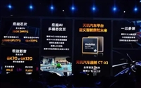
 联发科推出全球首款3纳米汽车芯片CT-X1,挑战高通SA8295

 国家大基金减持三家半导体企业,市场反应各异

 晶圆厂易主:Coherent公司2000万英镑出售苹果供应链关键资产
