
 5秒后页面跳转

| 是否无铅: | 不含铅 | 生命周期: | Active |
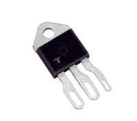
| 零件包装代码: | DFN | 包装说明: | SMALL OUTLINE, S-XDSO-N3 |
| 针数: | 3 | Reach Compliance Code: | compliant |
| ECCN代码: | EAR99 | Factory Lead Time: | 1 week |
| 风险等级: | 1.55 | 外壳连接: | COLLECTOR |
| 最大集电极电流 (IC): | 5 A | 集电极-发射极最大电压: | 20 V |
| 配置: | SINGLE | 最小直流电流增益 (hFE): | 180 |
| JESD-30 代码: | S-XDSO-N3 | JESD-609代码: | e3 |
| 湿度敏感等级: | 1 | 元件数量: | 1 |
| 端子数量: | 3 | 最高工作温度: | 150 °C |
| 封装主体材料: | UNSPECIFIED | 封装形状: | SQUARE |
| 封装形式: | SMALL OUTLINE | 峰值回流温度(摄氏度): | NOT SPECIFIED |
| 极性/信道类型: | PNP | 最大功率耗散 (Abs): | 1.5 W |
| 认证状态: | Not Qualified | 子类别: | Other Transistors |
| 表面贴装: | YES | 端子面层: | Tin (Sn) |
| 端子形式: | NO LEAD | 端子位置: | DUAL |
| 处于峰值回流温度下的最长时间: | NOT SPECIFIED | 晶体管应用: | SWITCHING |
| 晶体管元件材料: | SILICON | 标称过渡频率 (fT): | 100 MHz |
| 最大关闭时间(toff): | 510 ns | 最大开启时间(吨): | 235 ns |
| Base Number Matches: | 1 |
| 型号 | 品牌 | 替代类型 | 描述 | 数据表 |
| NSS20200W6T1G | ONSEMI |
功能相似  |
20 V, 3.0 A, Low VCE(sat) PNP Transistor |

|
| 型号 | 品牌 | 获取价格 | 描述 | 数据表 |
| NSS20500UW3T2G_07 | ONSEMI |
获取价格 |
20 V, 7.0 A, Low VCE(sat) PNP Transistor |
|
| NSS20500UW3TBG | ONSEMI |
获取价格 |
PNP Transistor |
|
| NSS20501UW3 | ONSEMI |
获取价格 |
NPN Transistor |
|
| NSS20501UW3T2G | ONSEMI |
获取价格 |
20 V, 7.0 A, Low VCE(sat) NPN Transistor |
|
| NSS20501UW3TBG | ONSEMI |
获取价格 |
NPN Transistor |
|
| NSS20600CF8T1G | ONSEMI |
获取价格 |
20 V, 7.0 A, Low VCE(sat) PNP Transistor |
|
| NSS20600CF8T1G_07 | ONSEMI |
获取价格 |
20 V, 7.0 A, Low VCE(sat) PNP Transistor |
|
| NSS20601CF8T1G | ONSEMI |
获取价格 |
20 V, 8.0 A, Low VCE(sat) NPN Transistor |
|
| NSS3 | COOPER |
获取价格 |
Barrier Strip Terminal Block, 30A, 1 Row(s), 1 Deck(s), |
|
| NSS30070MR6T1G | ONSEMI |
获取价格 |
30 V, 0.7 A, Low VCE(sat) PNP Transistor |
|
 晶闸管的静态特性与伏安特性详解

 贴片电容的工作原理与参数识别
 精密电路设计中的高精电阻:分流电阻
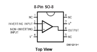 LM7131ACM5手册详解:微型高速单电源运算放大器的深度剖析
工作时间:9:00-21:00
CEO邮箱:ceo@jiepei.com
投诉邮箱:tousu@jiepei.com


 浙公网安备 33010502006866号 浙ICP备10014259号-119
营业执照ICP证
浙公网安备 33010502006866号 浙ICP备10014259号-119
营业执照ICP证


