
| 是否Rohs认证: | 符合 | 生命周期: | Transferred |
| 包装说明: | , | Reach Compliance Code: | unknown |
| 风险等级: | 5.61 | Is Samacsys: | N |
| 湿度敏感等级: | 1 | Base Number Matches: | 1 |
| 型号 | 品牌 | 获取价格 | 描述 | 数据表 |
| AAT7357_05 | ANALOGICTECH |
获取价格 |
20V P-Channel Power MOSFET |

|
| AAT7361 | ANALOGICTECH |
获取价格 |
20V P-Channel Power MOSFET |
|
| AAT7361ITS-T1 | ANALOGICTECH |
获取价格 |
20V P-Channel Power MOSFET |
|
| AAT7551 | ANALOGICTECH |
获取价格 |
20V P-Channel Power MOSFET |
|
| AAT7551IJS-T1 | ANALOGICTECH |
获取价格 |
20V P-Channel Power MOSFET |
|
| AAT8107 | ANALOGICTECH |
获取价格 |
20V P-Channel Power MOSFET |
|
| AAT8107IAS-T1 | ANALOGICTECH |
获取价格 |
20V P-Channel Power MOSFET |
|
| AAT8303 | ANALOGICTECH |
获取价格 |
20V P-Channel Power MOSFET |
|
| AAT8303ITS-T1 | ANALOGICTECH |
获取价格 |
20V P-Channel Power MOSFET |
|
| AAT8303_05 | ANALOGICTECH |
获取价格 |
20V P-Channel Power MOSFET |
|
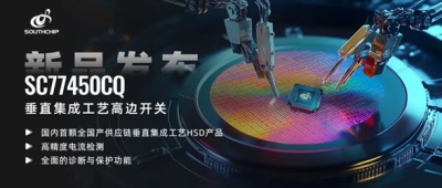 国产芯片新突破!南芯科技发布首颗全国产垂直集成高边开关

 美方收取15%在华收入分成!英伟达AMD获批对华出口AI芯片
 高性能计算推动封装革新:斥资20亿,国内半导体企业加快布局
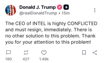 特朗普为何要求英特尔CEO陈立武立即辞职?利益冲突引股价震荡
工作时间:9:00-21:00
CEO邮箱:ceo@jiepei.com
投诉邮箱:tousu@jiepei.com


 浙公网安备 33010502006866号 浙ICP备10014259号-119
营业执照ICP证
浙公网安备 33010502006866号 浙ICP备10014259号-119
营业执照ICP证


