
 5秒后页面跳转

| 是否无铅: | 含铅 | 是否Rohs认证: | 符合 |
| 生命周期: | Active | 包装说明: | VFBGA, |
| 针数: | 16 | Reach Compliance Code: | compliant |
| 风险等级: | 5.67 | 其他特性: | OUTPUT VOLTAGE RANGE FROM 0.8 TO 5.2 VOLT AND 0.8V TO 3.8V FOR LDO |
| 模拟集成电路 - 其他类型: | DUAL SWITCHING CONTROLLER | 控制模式: | CURRENT-MODE |
| 控制技术: | PULSE WIDTH MODULATION | 最大输入电压: | 5.5 V |
| 最小输入电压: | 2.3 V | 标称输入电压: | 3.6 V |
| JESD-30 代码: | S-PBGA-B16 | JESD-609代码: | e1 |
| 长度: | 2 mm | 湿度敏感等级: | 1 |
| 功能数量: | 1 | 端子数量: | 16 |
| 最高工作温度: | 125 °C | 最低工作温度: | -40 °C |
| 封装主体材料: | PLASTIC/EPOXY | 封装代码: | VFBGA |
| 封装形状: | SQUARE | 封装形式: | GRID ARRAY, VERY THIN PROFILE, FINE PITCH |
| 峰值回流温度(摄氏度): | 260 | 座面最大高度: | 0.66 mm |
| 表面贴装: | YES | 切换器配置: | BUCK |
| 温度等级: | AUTOMOTIVE | 端子面层: | Tin/Silver/Copper (Sn/Ag/Cu) |
| 端子形式: | BALL | 端子节距: | 0.5 mm |
| 端子位置: | BOTTOM | 处于峰值回流温度下的最长时间: | 30 |
| 宽度: | 2 mm | Base Number Matches: | 1 |
| 型号 | 品牌 | 获取价格 | 描述 | 数据表 |
| ADP5033ACBZ-8-R7 | ADI |
获取价格 |
Dual 3 MHz, 800 mA Buck Regulators with Two 300 mA LDOs |

|
| ADP5033ACBZ-9-R7 | ADI |
获取价格 |
Dual 3 MHz, 800 mA Buck Regulators with Two 300 mA LDOs |
|
| ADP5034 | ADI |
获取价格 |
Dual 3 MHz, 1200 mA Buck Regulators with Two 300 mA LDOs |
|
| ADP5034-1-EVALZ | ADI |
获取价格 |
Dual 3 MHz, 1200 mA Buck Regulators with Two 300 mA LDOs |
|
| ADP5034-2-EVALZ | ADI |
获取价格 |
Dual 3 MHz, 1200 mA Buck Regulators with Two 300 mA LDOs |
|
| ADP5034ACPZ-1-R7 | ADI |
获取价格 |
Dual 3 MHz, 1200 mA Buck Regulators with Two 300 mA LDOs |
|
| ADP5034ACPZ-2-R7 | ADI |
获取价格 |
Dual 3 MHz, 1200 mA Buck Regulators with Two 300 mA LDOs |
|
| ADP5034ACPZ-3-R7 | ADI |
获取价格 |
Dual 3 MHz, 1200mA Buck Regulator with Two 300 mA LDOs |
|
| ADP5034ACPZ-R2 | ADI |
获取价格 |
Dual 3 MHz, 1200mA Buck Regulator with Two 300 mA LDOs |
|
| ADP5034ACPZ-R7 | ADI |
获取价格 |
Dual 3 MHz, 1200 mA Buck Regulators with Two 300 mA LDOs |
|
 MAX232IDR数据手册:产品特性、电气参数、替代型号推荐

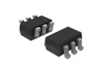 2N7002DW数据手册:参数解读、引脚信息、替代型号推荐
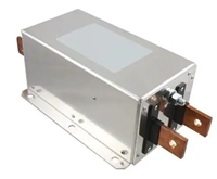 网络滤波器、EMI滤波器与EMC滤波器在电子元器件中的分类关系
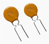 NTC热敏电阻与PTC热敏电阻的应用原理及选型原则
工作时间:9:00-21:00
CEO邮箱:ceo@jiepei.com
投诉邮箱:tousu@jiepei.com


 浙公网安备 33010502006866号 浙ICP备10014259号-119
营业执照ICP证
浙公网安备 33010502006866号 浙ICP备10014259号-119
营业执照ICP证


