
| 生命周期: | Active | 零件包装代码: | SON |
| 包装说明: | VSON, | 针数: | 6 |
| Reach Compliance Code: | compliant | HTS代码: | 8542.39.00.01 |
| 风险等级: | 1.28 | 系列: | LVC/LCX/Z |
| JESD-30 代码: | S-PDSO-N6 | JESD-609代码: | e3 |
| 长度: | 1 mm | 逻辑集成电路类型: | INVERTER |
| 湿度敏感等级: | 1 | 功能数量: | 2 |
| 输入次数: | 1 | 端子数量: | 6 |
| 最高工作温度: | 125 °C | 最低工作温度: | -40 °C |
| 封装主体材料: | PLASTIC/EPOXY | 封装代码: | VSON |
| 封装形状: | SQUARE | 封装形式: | SMALL OUTLINE, VERY THIN PROFILE |
| 峰值回流温度(摄氏度): | 260 | 传播延迟(tpd): | 12 ns |
| 认证状态: | Not Qualified | 座面最大高度: | 0.5 mm |
| 最大供电电压 (Vsup): | 5.5 V | 最小供电电压 (Vsup): | 1.65 V |
| 标称供电电压 (Vsup): | 1.8 V | 表面贴装: | YES |
| 技术: | CMOS | 温度等级: | AUTOMOTIVE |
| 端子面层: | Tin (Sn) | 端子形式: | NO LEAD |
| 端子节距: | 0.35 mm | 端子位置: | DUAL |
| 处于峰值回流温度下的最长时间: | 30 | 宽度: | 1 mm |
| Base Number Matches: | 1 |
| 型号 | 品牌 | 替代类型 | 描述 | 数据表 |
| 74LVC2G14GM,115 | NXP |
功能相似  |
74LVC2G14 - Dual inverting Schmitt trigger with 5 V tolerant input SON 6-Pin |

|
| 74LVC2G14GM,132 | NXP |
功能相似 |
74LVC2G14 - Dual inverting Schmitt trigger with 5 V tolerant input SON 6-Pin |
|
| 74LVC2G14GM | NEXPERIA |
功能相似 |
Dual inverting Schmitt trigger with 5 V tolerant inputProduction |
|
| 型号 | 品牌 | 获取价格 | 描述 | 数据表 |
| 74LVC2G14GM | NXP |
获取价格 |
Dual inverting Schmitt-trigger with 5 V tolerant input |
|
| 74LVC2G14GM | NEXPERIA |
获取价格 |
Dual inverting Schmitt trigger with 5 V tolerant inputProduction |
|
| 74LVC2G14GM,115 | NXP |
获取价格 |
74LVC2G14 - Dual inverting Schmitt trigger with 5 V tolerant input SON 6-Pin |
|
| 74LVC2G14GM,132 | NXP |
获取价格 |
74LVC2G14 - Dual inverting Schmitt trigger with 5 V tolerant input SON 6-Pin |
|
| 74LVC2G14GM-Q100 | NEXPERIA |
获取价格 |
Dual inverting Schmitt trigger with 5 V tolerant input |
|
| 74LVC2G14GN | NEXPERIA |
获取价格 |
Dual inverting Schmitt trigger with 5 V tolerant inputProduction |
|
| 74LVC2G14GS | NEXPERIA |
获取价格 |
Dual inverting Schmitt trigger with 5 V tolerant inputProduction |
|
| 74LVC2G14GV | NXP |
获取价格 |
Dual inverting Schmitt-trigger with 5 V tolerant input |
|
| 74LVC2G14GV | NEXPERIA |
获取价格 |
Dual inverting Schmitt trigger with 5 V tolerant inputProduction |
|
| 74LVC2G14GV,125 | NXP |
获取价格 |
74LVC2G14 - Dual inverting Schmitt trigger with 5 V tolerant input TSOP 6-Pin |
|
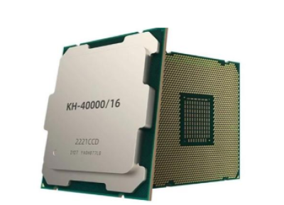 国产x86处理器里程碑!兆芯6000台医疗电脑中标某总医院

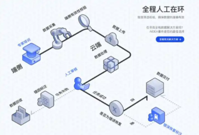 稚晖君团队开源GO-1模型:ViLLA架构如何重塑具身智能未来?
 安森美收购奥拉半导体Vcore技术 抢占AI数据中心电源管理制高点
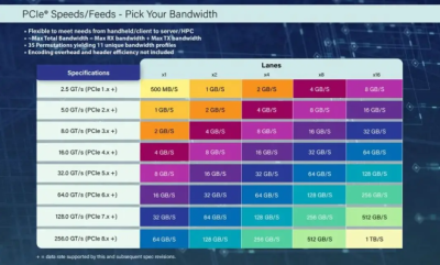 PCIe 8.0规范草案获里程碑进展:256GT/s速率开启1TB/s带宽时代
工作时间:9:00-21:00
CEO邮箱:ceo@jiepei.com
投诉邮箱:tousu@jiepei.com


 浙公网安备 33010502006866号 浙ICP备10014259号-119
营业执照ICP证
浙公网安备 33010502006866号 浙ICP备10014259号-119
营业执照ICP证


