VITESSE
SEMICONDUCTOR CORPORATION
Datasheet
2.5 Gbits/sec
34x34 Crosspoint Switch with Signal Detection
VSC835
Features
• 34 Input by 34 Output Crosspoint Switch
• 50Ω Source Terminated PECL Output Drivers
• Single 3.3V Supply
• 2.5 Gbits/sec. NRZ Data Bandwidth
• TTL Compatible µP Interface
• Differential PECL Data Inputs
• On-chip 50Ω Input Terminations
• 14W Maximum Power Dissipation
• High Performance 256 BGA Package
General Description
The VSC835 is a monolithic 34x34 asynchronous crosspoint switch, designed to carry broadband data
streams at up to 2.5 Gbit/s. The non-blocking switch core is programmed through a parallel port interface that
allows random access programming of each output port. A high degree of signal integrity is maintained through
the chip through fully differential signal paths.
The crosspoint function is based on a multiplexer tree architecture. Each data output is driven by a 34:1
multiplexer tree that can be programmed to one and only one of its 34 inputs, and each data input can be routed
to multiple outputs. The signal path is unregistered, so no clock is required for the data inputs. The signal path is
asynchronous, so there are no restrictions on the phase, frequency, or signal pattern at each input. Each input
channel and each output channel has an signal monitor function that can be used to identify loss of activity
(LOA). An interrupt pin is provided to signal LOA, after which an external controller can query the chip to
determine the channel(s) on which the fault occurred.
Each output driver is a fully differential switched current driver with on-die back-terminations for maxi-
mum signal integrity. Data inputs are terminated on die through 50 ohm resistors terminated to V
.
TERM
The parallel interface uses TTL levels, and provides address, data, and control pins that are compatible
with a microprocessor-style interface. The control port provides access to all chip functions, including LOA and
programming. Program buffering is provided to allow multiple program assignments to be queued and issued
simultaneously via a single configure command.
VSC835 Block Diagram
A0
Y0
A33
Y33
Control Logic
µP interface
G52270-0, Rev. 4.1
7/24/00
VITESSE SEMICONDUCTOR CORPORATION
741 Calle Plano, Camarillo, CA 93012 • 805/388-3700 • FAX: 805/987-5896
Page 1


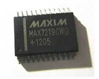
 MAX7219驱动8段数码管详解及数据手册关键信息

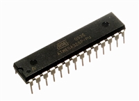
 ATMEGA328P技术资料深入分析

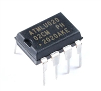
 AT24C02芯片手册管脚信息、参数分析、应用领域详解

 AT24C256芯片手册参数分析、引脚说明、读写程序示例
