VSC838-01
Datasheet
3.2 Gbps 36 × 36 Crosspoint Switch
Features
•
•
•
36 inputs by 36 outputs
•
•
•
•
•
Parallel and serial programming modes
Programmable on-chip I/O termination
Differential CML output drivers
Single 2.5 V supply
3.2 Gbps NRZ data bandwidth
Non-blocking architecture broadcast and multicast
capabilities
•
•
•
LVTTL/2.5 V CMOS control I/O (3.3 V tolerant)
Input signal activity (ISA) monitoring function
6 W typical, Low-Drive mode
7 W typical, High-Drive mode
Integrated signal equalization (ISE) for
deterministic jitter reduction
•
37.5 mm, 480-pin TBGA package
•
66 MHz dual programming port
General Description
The VSC838-01 device is a monolithic, 36 by 36, asynchronous crosspoint switch designed to carry broadband data
streams. It has an internal 37th output channel which is used in conjunction with the Input Signal Activity (ISA)
monitoring function to facilitate efficient system diagnostics. A high degree of signal integrity is maintained
throughout the chip by means of fully differential signal paths.
The device crosspoint function is based on a multiplexer array architecture. Each data output is driven by a 36:1
multiplexer that can be programmed to one, and only one of its 36 inputs. The signal path is unregistered and fully
asynchronous, so there are no restrictions on the phase, frequency, or signal pattern at each input.
Each high-speed output is a fully differential, switched current driver with switchable on-die terminations for
maximum signal integrity. Data inputs are terminated on-die using 100 Ω impedance between true and complement
inputs. For more information, see “Input Terminations,” page 9.
A dual mode programming interface is provided that allows programming commands to be sent as serial data or
parallel data. Core programming can be random for each port address, or multiple program assignments can be
queued and issued simultaneously. The programming may be initialized to a “straight-through” configuration (A0 to
Y0, A1 to Y1, etc.) using the INIT pin.
VMDS-10195 Revision 4.0
© VITESSE SEMICONDUCTOR CORPORATION • 741 Calle Plano • Camarillo, CA 93012
Tel: (800) VITESSE • FAX: (805) 987-5896 • Email: prodinfo@vitesse.com
Internet: www.vitesse.com
1 of 19
August 19, 2005


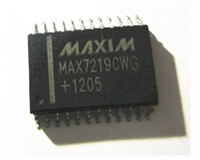
 MAX7219驱动8段数码管详解及数据手册关键信息

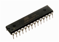
 ATMEGA328P技术资料深入分析

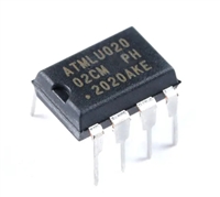
 AT24C02芯片手册管脚信息、参数分析、应用领域详解

 AT24C256芯片手册参数分析、引脚说明、读写程序示例
