
 5秒后页面跳转

| 型号 | 品牌 | 获取价格 | 描述 | 数据表 |
| HD74CDC2510BTEL | RENESAS |
获取价格 |
3.3-V Phase-lock Loop Clock Driver |

|
| HD74CDC587 | HITACHI |
获取价格 |
PLL Based Clock Driver, CDC Series, CMOS, PDSO56, TTP-56D |
|
| HD74CDC857 | HITACHI |
获取价格 |
3.3/2.5-V Phase-lock Loop Clock Driver |
|
| HD74CDCF2509B | RENESAS |
获取价格 |
140 MHz, 0 to 85°C Operation 3.3-V Phase-lock |
|
| HD74CDCF2509B | HITACHI |
获取价格 |
140 MHz, 0 to 85∑C Operation 3.3-V Phase-lock |
|
| HD74CDCF2509BT | RENESAS |
获取价格 |
暂无描述 |
|
| HD74CDCF2509BTEL | RENESAS |
获取价格 |
140 MHz, 0 to 85°C Operation 3.3-V Phase-lock |
|
| HD74CDCF2510B | HITACHI |
获取价格 |
140 MHz, 0 to 85∑C Operation 3.3-V Phase-lock |
|
| HD74CDCF2510BT | HITACHI |
获取价格 |
PLL Based Clock Driver, CDCF Series, 10 True Output(s), 0 Inverted Output(s), PDSO24, TTP- |
|
| HD74CDCF2510BTEL | HITACHI |
获取价格 |
PLL Based Clock Driver, CDCF Series, 10 True Output(s), 0 Inverted Output(s), PDSO24, TTP- |
|
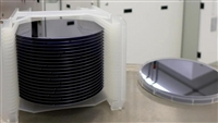 晶圆厂易主:Coherent公司2000万英镑出售苹果供应链关键资产

 Galaxy S25系列或全系搭载骁龙8 Elite
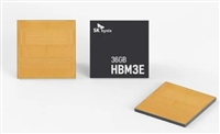 三大厂商12层HBM3E进展迅速
 塔塔电子与力积电达成技术转让协议,携手建设印度首座晶圆厂
工作时间:9:00-21:00
CEO邮箱:ceo@jiepei.com
投诉邮箱:tousu@jiepei.com


 浙公网安备 33010502006866号 浙ICP备10014259号-119
营业执照ICP证
浙公网安备 33010502006866号 浙ICP备10014259号-119
营业执照ICP证


