9DBL02 DATASHEET
Electrical Characteristics–DIF Low-Power HCSL Outputs
TA = TAMB, Supply Voltages per normal operation conditions, See Test Loads for Loading Conditions
PARAMETER
Slew rate
SYMBOL
CONDITIONS
MIN
TYP MAX UNITS NOTES
V/ns
V/ns
%
dV/dt
dV/dt
Scope averaging on, fast setting
Scope averaging on, slow setting
Slew rate matching
2
1.2
2.8
1.9
7
4
3.1
20
1,2,3
1,2,3
1,2,4
Slew rate matching
Voltage High
dV/dt
Δ
Statistical measurement on single-ended signal
using oscilloscope math function. (Scope
averaging on)
VHIGH
660
768
-11
850
7
7
mV
Voltage Low
VLOW
-150
150
Max Voltage
Min Voltage
Crossing Voltage (abs)
Crossing Voltage (var)
Vmax
Vmin
Vcross_abs
Measurement on single ended signal using
absolute value. (Scope averaging off)
Scope averaging off
811
-49
357
14
1150
7
7
1,5
1,6
mV
-300
250
550
140
mV
mV
-Vcross
Scope averaging off
Δ
1Guaranteed by design and characterization, not 100% tested in production.
2 Measured from differential waveform
3 Slew rate is measured through the Vswing voltage range centered around differential 0V. This results in a +/-150mV window around
differential 0V.
4 Matching applies to rising edge rate for Clock and falling edge rate for Clock#. It is measured using a +/-75mV window centered on
the average cross point where Clock rising meets Clock# falling. The median cross point is used to calculate the voltage thresholds the
oscilloscope is to use for the edge rate calculations.
5 Vcross is defined as voltage where Clock = Clock# measured on a component test board and only applies to the differential rising
edge (i.e. Clock rising and Clock# falling).
6 The total variation of all Vcross measurements in any particular system. Note that this is a subset of Vcross_min/max (Vcross
absolute) allowed. The intent is to limit Vcross induced modulation by setting -Vcross to be smaller than Vcross absolute.
Δ
7 At default SMBus settings.
Electrical Characteristics–Current Consumption
TA = TAMB, Supply Voltages per normal operation conditions, See Test Loads for Loading Conditions
PARAMETER
SYMBOL
IDDA
CONDITIONS
MIN
TYP
7
MAX
10
UNITS NOTES
VDDA, PLL Mode @100MHz
VDDDIG, PLL Mode @100MHz
mA
mA
mA
Operating Supply Current
IDDDIG
3.4
5
IDDO+R
VDDO+VDDR, PLL Mode, All outputs @100MHz
VDDA, CKPWRGD_PD# = 0
20
0.6
3.0
0.9
25
1.0
4.3
1.3
IDDRPD
IDDDIGPD
IDDAOPD
mA
mA
mA
1
1
1
Powerdown Current
VDDDIG, CKPWRGD_PD# = 0
VDDO+VDDR, CKPWRGD_PD# = 0
1 Input clock stopped.
OCTOBER 6, 2016
7
2-OUTPUT 3.3V PCIE ZERO-DELAY BUFFER


 MAX6675资料手册参数详解、引脚配置说明

 LM258引脚图及功能介绍、主要参数分析

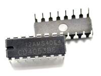
 CD4052资料手册参数详解、引脚配置说明

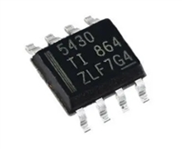
 一文带你了解TPS5430资料手册分析:参数介绍、引脚配置说明
