
 5秒后页面跳转

| 型号 | 品牌 | 获取价格 | 描述 | 数据表 |
| CY7C1299A-100AC | CYPRESS |
获取价格 |
32K x 36 Dual I/O Dual Address Synchronous SRAM |

|
| CY7C1299A-83AC | CYPRESS |
获取价格 |
32K x 36 Dual I/O Dual Address Synchronous SRAM |
|
| CY7C129DV18 | CYPRESS |
获取价格 |
RAM9 QDR-I/DDR-I/QDR-II/DDR- II Errata |
|
| CY7C129EV18 | CYPRESS |
获取价格 |
RAM9 QDR-I/DDR-I/QDR-II/DDR- II Errata |
|
| CY7C130 | CYPRESS |
获取价格 |
1K x 8 Dual-Port Static Ram |
|
| CY7C130*BV18 | CYPRESS |
获取价格 |
RAM9 QDR-I/DDR-I/QDR-II/DDR- II Errata |
|
| CY7C130*BV25 | CYPRESS |
获取价格 |
RAM9 QDR-I/DDR-I/QDR-II/DDR- II Errata |
|
| CY7C130*DV25 | CYPRESS |
获取价格 |
RAM9 QDR-I/DDR-I/QDR-II/DDR- II Errata |
|
| CY7C130_05 | CYPRESS |
获取价格 |
1K x 8 Dual-Port Static RAM |
|
| CY7C130_12 | CYPRESS |
获取价格 |
1 K Ã 8 Dual-Port Static RAM |
|
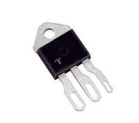 晶闸管的静态特性与伏安特性详解

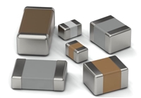 贴片电容的工作原理与参数识别
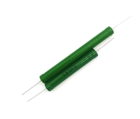 精密电路设计中的高精电阻:分流电阻
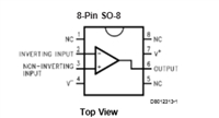 LM7131ACM5手册详解:微型高速单电源运算放大器的深度剖析
工作时间:9:00-21:00
CEO邮箱:ceo@jiepei.com
投诉邮箱:tousu@jiepei.com


 浙公网安备 33010502006866号 浙ICP备10014259号-119
营业执照ICP证
浙公网安备 33010502006866号 浙ICP备10014259号-119
营业执照ICP证


