VITESSE
SEMICONDUCTOR CORPORATION
Preliminary Datasheet
STS-48c Packet/ATM Over SONET/SDH Device
With Integrated Mux/Demux and Clock and Data Recovery
VSC9142
43
• The 48 byte information field is scrambled with a self-synchronizing descrambler polynomial 1 + x .
Scrambling can be enabled/disabled.
• The HEC generator performs a CRC-8 calculation over the first four header octets using the generating
2
8
2
4
6
polynomial 1 + x + x + x . The coset polynomial 1 + x + x +x can be added to the result. The HEC
is optionally inserted into the fifth octet of the header of cells read from the Tx FIFO.
• The Tx FIFO can accomodate storage of eight ATM cells.
Transmit Packet Processor (TPP)
• The inserted HDLC Flag Sequence byte and the minimum number of Flag Sequence bytes separating
HDLC frames are programmable.
• The insertion of the Address and Control fields can be controlled by the HDLC Address-and-Control-
Field-Compression mechanism.
• The Address Field inserted after the beginning Flag Sequence is programmable.
• The Control Field inserted after the the Address Field is programmable.
• The Frame Check Sequence (FCS) can be generated using either a 16-bit, CRC-CCITT generating poly-
5
12
16
2
4
5
7
8
10
nomial 1 + x + x + x , or a 32-bit CRC-32 generating polynomial 1 + x + x + x + x + x + x + x
11
12
16
22
23
26
32
+ x + x + x + x + x + x + x .
• Octet Stuffing, or “escaping”, can be applied after the FCS generation and partial scrambling, if enabled.
The Control Escape byte and the Octet Stuffing Masking byte are programmable. The Asyc-Control-
Character-Map (ACCM) can accommodate a maximum of 5 byte values. Each value can be individually
enabled/disabled.
43
• The transmitted data is scrambled with a self-synchronizing scrambler (SSS) polynomial 1 + x . Full
and/or partial scrambling can be independently enabled/disabled.
• The PPP Protocol Field can be generated internally or extracted from the transmit FIFO. The size and
value of the inserted Protocol Field are programmable when generated internally.
• The Tx FIFO is programmable in the range from 1 to 4095 words or 16380 bytes of data storage. All
valid packet bytes stored in the Tx FIFO are read out and mapped into the PPP Protocol/Information
Fields of generated PPP/HDLC frames.
• Two Tx PIF packet transfer modes are supported: packet transfer mode and word transfer mode.
• The TXF_ERR signal is provided to force insertion of errors into the FCS, or to force abort the transmit-
ted HDLC frame.
• It is possible to force XOR'ing of the transmitted Address, Control or Protocol Fields with a programma-
ble mask value via the CPU interface for diagnostic purposes.
• The following statistics are provided in the performance monitoring 32-bit counters:
• Bytes read from Tx FIFO
• Transmitted good HDLC frames (non-aborted, non-FCS errored)
G52319-0, Rev. 3.1
VITESSE SEMICONDUCTOR CORPORATION
Page 7
6/12/00
741 Calle Plano, Camarillo, CA 93012 • 805/388-3700 • FAX: 805/987-5896


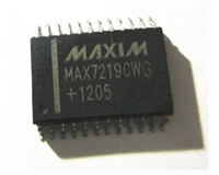
 MAX7219驱动8段数码管详解及数据手册关键信息

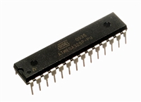
 ATMEGA328P技术资料深入分析

 AT24C02芯片手册管脚信息、参数分析、应用领域详解

 AT24C256芯片手册参数分析、引脚说明、读写程序示例
