
 5秒后页面跳转

| 是否Rohs认证: | 符合 | 生命周期: | Active |
| 包装说明: | , | Reach Compliance Code: | unknown |
| 风险等级: | 5.8 | 最大集电极电流 (IC): | 0.1 A |
| 最小直流电流增益 (hFE): | 120 | 元件数量: | 2 |
| 极性/信道类型: | NPN | 最大功率耗散 (Abs): | 0.1 W |
| 子类别: | BIP General Purpose Small Signal | 表面贴装: | YES |
| 晶体管元件材料: | SILICON | Base Number Matches: | 1 |
| 型号 | 品牌 | 获取价格 | 描述 | 数据表 |
| RN1910FS | TOSHIBA |
获取价格 |
Switching, Inverter Circuit, Interface Circuit and Driver Circuit Applications |

|
| RN1910FS(TPL3) | TOSHIBA |
获取价格 |
PRE-BIASED "DIGITAL" TRANSISTOR,20V V(BR)CEO,50MA I(C),TSOP |
|
| RN1910TE85L | TOSHIBA |
获取价格 |
TRANSISTOR 100 mA, 50 V, 2 CHANNEL, NPN, Si, SMALL SIGNAL TRANSISTOR, BIP General Purpose |
|
| RN1910TE85N | TOSHIBA |
获取价格 |
TRANSISTOR 100 mA, 50 V, 2 CHANNEL, NPN, Si, SMALL SIGNAL TRANSISTOR, BIP General Purpose |
|
| RN1910TE85R | TOSHIBA |
获取价格 |
TRANSISTOR 100 mA, 50 V, 2 CHANNEL, NPN, Si, SMALL SIGNAL TRANSISTOR, BIP General Purpose |
|
| RN1911 | TOSHIBA |
获取价格 |
Switching, Inverter Circuit, Interface Circuit And Driver Circuit Applications |
|
| RN1911(TE85L) | TOSHIBA |
获取价格 |
TRANSISTOR 100 mA, 50 V, 2 CHANNEL, NPN, Si, SMALL SIGNAL TRANSISTOR, BIP General Purpose |
|
| RN1911(TE85L,F) | TOSHIBA |
获取价格 |
PRE-BIASED "DIGITAL" TRANSISTOR,50V V(BR)CEO,100MA I(C),TSOP |
|
| RN1911(TE85R) | TOSHIBA |
获取价格 |
TRANSISTOR 100 mA, 50 V, 2 CHANNEL, NPN, Si, SMALL SIGNAL TRANSISTOR, US6, 2-2J1A, 6 PIN, |
|
| RN1911,LF(CT | TOSHIBA |
获取价格 |
Small Signal Bipolar Transistor |
|
 AP1152ADU51资料手册解读:低压差线性稳压器的全面剖析

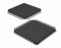 MB91F223S 微控制器详解:全方位解读其数据手册
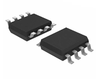 DS1135-8资料手册解读:深入探索高速硅定时电路的特性与应用
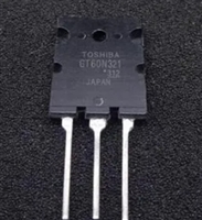 GT60N321资料手册解读:深入了解东芝第四代绝缘栅双极晶体管
工作时间:9:00-21:00
CEO邮箱:ceo@jiepei.com
投诉邮箱:tousu@jiepei.com


 浙公网安备 33010502006866号 浙ICP备10014259号-119
营业执照ICP证
浙公网安备 33010502006866号 浙ICP备10014259号-119
营业执照ICP证


