
 5秒后页面跳转

| 是否无铅: | 不含铅 | 生命周期: | Active |
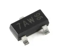
| 包装说明: | SMALL OUTLINE, R-PDSO-G3 | 针数: | 3 |
| Reach Compliance Code: | compliant | ECCN代码: | EAR99 |
| Factory Lead Time: | 8 weeks | 风险等级: | 1.54 |
| 最大集电极电流 (IC): | 2 A | 集电极-发射极最大电压: | 60 V |
| 配置: | SINGLE | 最小直流电流增益 (hFE): | 100 |
| JEDEC-95代码: | TO-236AB | JESD-30 代码: | R-PDSO-G3 |
| JESD-609代码: | e3 | 湿度敏感等级: | 1 |
| 元件数量: | 1 | 端子数量: | 3 |
| 封装主体材料: | PLASTIC/EPOXY | 封装形状: | RECTANGULAR |
| 封装形式: | SMALL OUTLINE | 峰值回流温度(摄氏度): | NOT SPECIFIED |
| 极性/信道类型: | NPN | 表面贴装: | YES |
| 端子面层: | Tin (Sn) | 端子形式: | GULL WING |
| 端子位置: | DUAL | 处于峰值回流温度下的最长时间: | NOT SPECIFIED |
| 晶体管应用: | SWITCHING | 晶体管元件材料: | SILICON |
| 标称过渡频率 (fT): | 100 MHz | 最大关闭时间(toff): | 1220 ns |
| 最大开启时间(吨): | 155 ns | Base Number Matches: | 1 |
| 型号 | 品牌 | 替代类型 | 描述 | 数据表 |
| NSS60201LT1G | ONSEMI |
类似代替  |
60 V, 4.0 A, Low VCE(sat) NPN Transistor |

|
| 型号 | 品牌 | 获取价格 | 描述 | 数据表 |
| NSV60201SMTWTBG | ONSEMI |
获取价格 |
Single 60V 2A Low VCE(sat) NPN Transistor in WDFN6 |
|
| NSV60600MZ4T1G | ONSEMI |
获取价格 |
60 V, 6.0 A, Low VCE(sat) PNP Transistor |
|
| NSV60600MZ4T3G | ONSEMI |
获取价格 |
60 V, 6.0 A, Low VCE(sat) PNP Transistor |
|
| NSV60601MZ4T1G | ONSEMI |
获取价格 |
60 V, 6.0 A, Low VCE(sat) NPN Transistor |
|
| NSV60601MZ4T3G | ONSEMI |
获取价格 |
60 V, 6.0 A, Low VCE(sat) NPN Transistor |
|
| NSV9435T1G | ONSEMI |
获取价格 |
PNP 双极数字晶体管 (BRT) |
|
| NSVA207 | NJRC |
获取价格 |
SAW Filter, |
|
| NSVA208 | NJRC |
获取价格 |
SAW Filter, |
|
| NSVA253 | NJRC |
获取价格 |
SAW Filter, 1 Function(s), 1216.5MHz, |
|
| NSVA254 | NJRC |
获取价格 |
SAW Filter, 1 Function(s), 1252.5MHz, |
|
 压敏电阻与气体放电管串联使用的专业解析

 手册解读:MMBT3904参数与管脚图及代换
 74LS298PC手册解读:参数说明、引脚说明、替代型号推荐
 L6234手册解读:引脚信息、电气参数
工作时间:9:00-21:00
CEO邮箱:ceo@jiepei.com
投诉邮箱:tousu@jiepei.com


 浙公网安备 33010502006866号 浙ICP备10014259号-119
营业执照ICP证
浙公网安备 33010502006866号 浙ICP备10014259号-119
营业执照ICP证


