DPA423-426
(typical), the CONTROL pin goes into the hysteretic mode of
operation. In this mode, the CONTROL pin goes through
alternate charge and discharge cycles between 4.8 V and 5.8 V
(see CONTROL Pin Operation section above) and the IC runs
entirely off the high voltage DC input, but with very low power
consumption (30 mW typical at 48 V with LINE-SENSE and
EXTERNAL CURRENT LIMIT pins open). When the
DPA-Switch is remotely turned on after entering this mode, it
will initiate a normal start-up sequence with soft-start the next
time the CONTROL pin reaches 5.8 V. In the worst case, the
delay from remote on to start-up can be equal to the full
discharge/charge cycle time of the CONTROL pin, which is
approximately 36 ms for a 22 µF CONTROL pin capacitor.
This reduced-consumption remote-off mode can eliminate
expensive and unreliable in-line mechanical switches. It also
allows for microprocessor-controlled turn-on and turn-off
sequences that may be required in certain applications.
hysteretic regulation of CONTROL pin voltage (VC), due to
remote off or thermal shutdown conditions. This effectively
minimizescurrentandvoltagestressesontheoutputMOSFET,
the clamp circuit and the output rectifier during start-up. This
feature also helps minimize output overshoot and prevents
saturation of the transformer during start-up.
Shutdown/Auto-Restart
To minimize DPA-Switch power dissipation under fault
conditions, the shutdown/auto-restart circuit turns the power
supply on and off at an auto-restart duty cycle of typically 4%
if an out of regulation condition persists. Loss of regulation
interrupts the external current into the CONTROL pin. VC
regulation changes from shunt mode to the hysteretic auto-
restart mode as described in CONTROL pin operation section.
When the fault condition is removed, the power supply output
becomes regulated, VC regulation returns to shunt mode, and
normal operation of the power supply resumes.
Synchronization
In addition to sensing incoming current for OV, UV and remote
ON/OFF, the LINE-SENSE pin also monitors its pin voltage
through a 1 V threshold comparator. A pin voltage below 1 V
turns on DPA-Switch. When the voltage at LINE-SENSE pin
rises beyond 1 V to disable the output, DPA-Switch completes
its current switching cycle before the output is forced off
(similar to remote ON/OFF operation). The internal oscillator
is stopped at the end of the current cycle awaiting the
LINE-SENSE pin voltage to go low to start the next cycle. This
allows the use of the 1 V threshold to synchronize DPA-Switch
to an external signal with a frequency lower than its internal
switching frequency. A transistor or an optocoupler output
connectedbetweentheLINE-SENSEpinandtheSOURCEpin
implements this function (see Figure 24). Please refer to
Figure6forthetimingwaveformsofsynchronizationoperation.
Hysteretic Over-Temperature Protection
Over temperature protection is provided by a precision analog
circuit that turns the output MOSFET off when the junction
temperature exceeds the thermal shutdown temperature
(137 °C typical). When the junction temperature cools to below
the hysteretic temperature (110 °C typical), normal operation
resumes providing automatic recovery. VC is regulated in
hysteretic mode and a 4.8 V to 5.8 V (typical) sawtooth
waveform is present on the CONTROL pin while in thermal
shutdown.
Bandgap Reference
All critical DPA-Switch internal voltages are derived from a
temperature-compensated bandgap reference. This reference is
also used to generate a temperature-compensated current
reference that is trimmed to accurately set the switching
frequency, current limit, and the line OV/UV thresholds.
DPA-Switchhas improved circuitry to maintain all of the above
critical parameters within very tight absolute and temperature
tolerances.
In order to be recognized as a synchronization pulse, the
LINE-SENSE pin needs to stay low (on-time) for at least
120 ns but no more than 2250 ns for 400 kHz (or 3080 ns for
300kHz)internalswitchingfrequency.Inaddition,theoff-time
mustbekeptbelow7.7µswhichisalimitationsetbythelowest
synchronizationfrequencyof128kHzallowedbythechip. The
effectiveDCMAXforsynchronizationoperationcanbecalculated
as0.75xfSYNC/fOSC. Anoff-timelongerthan7.7µsmayforcethe
CONTROLpintogointothehystereticmodeandinitiateasoft-
start cycle at next turn-on.
High-Voltage Bias Current Source
This current source biases DPA-Switch from the DRAIN pin
and charges the CONTROL pin external capacitance during
start-up or hysteretic operation. Hysteretic operation occurs
duringauto-restart,remoteoffandover-temperatureshutdown.
In this mode of operation, the current source is switched on and
off with an effective duty cycle of approximately 20%. This
duty cycle is determined by the ratio of CONTROL pin charge
(IC(CH)) and discharge currents (ICD1 and ICD2). This current
source is turned off during normal operation when the output
MOSFETisswitching.Theeffectofthecurrentsourceswitching
may be seen on the DRAIN voltage waveform as small
disturbances which is normal.
Soft-Start
Two on-chip soft-start functions are activated at start-up with a
duration of 5 ms (typical). Maximum duty cycle starts from 0%
andlinearlyincreasestothedefaultmaximumof75%attheend
of the 5 ms duration and the current limit starts from about 85%
and linearly increases to 100% at the end of the 5 ms duration.
In addition to start-up, soft-start is also activated at each restart
attempt during auto-restart and when restarting after being in
K
1/04
8


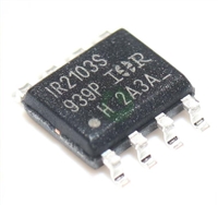
 深入解读IR2103资料手册:引脚说明、电气参数及替换型号推荐

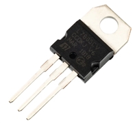
 L7805CV手册解读:引脚说明、替代型号推荐、好坏检测

 MMBT5551资料手册解读:电气参数、替换型号推荐

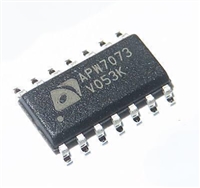
 APW7073资料手册解读:产品特性、引脚说明、替换型号推荐
