
 5秒后页面跳转

| 型号 | 品牌 | 获取价格 | 描述 | 数据表 |
| NSTB1005DXV5T1 | ONSEMI |
获取价格 |
Dual Common Base-Collector Bias Resistor Transistors |

|
| NSTB1005DXV5T1G | ONSEMI |
获取价格 |
Dual Common Base-Collector Bias Resistor Transistors |
|
| NSTB1005DXV5T5 | ONSEMI |
获取价格 |
Dual Common Base-Collector Bias Resistor Transistors |
|
| NSTB1010XV5T1 | ONSEMI |
获取价格 |
100mA, 50V, 2 CHANNEL, NPN AND PNP, Si, SMALL SIGNAL TRANSISTOR, CASE 463B-01, 5 PIN |
|
| NSTB1010XV5T5 | ONSEMI |
获取价格 |
100mA, 50V, 2 CHANNEL, NPN AND PNP, Si, SMALL SIGNAL TRANSISTOR, CASE 463B-01, 5 PIN |
|
| NSTB60ADW1T1/D | ETC |
获取价格 |
PNP General Purpose and NPN Bias Resistor Transistor Combination |
|
| NSTB60BDW1T1 | ONSEMI |
获取价格 |
PNP General Purpose and NPN Bias Resistor Transistor Combination |
|
| NSTB60BDW1T1/D | ONSEMI |
获取价格 |
PNP General Purpose and NPN Bias Resistor Transistor combination |
|
| NSTB60BDW1T1G | ONSEMI |
获取价格 |
PNP General Purpose and NPN Bias Resistor |
|
| NSTE184M63V76X142F | NICHICON |
获取价格 |
CAPACITOR, ALUMINUM ELECTROLYTIC, NON SOLID, POLARIZED, 63V, 180000uF, CHASSIS MOUNT, RADI |
|
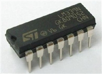 LM339N参数手册 :四路电压比较器的深度解读

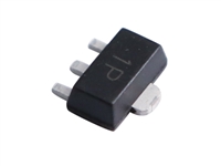 MMBT2222A资料手册:特性、应用、电气参数及替换型号推荐
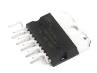 解读TDA7265手册资料:引脚说明 、电气参数及替换型号推荐
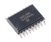 深入解读ULN2803A资料手册:引脚功能、电气参数、特性
工作时间:9:00-21:00
CEO邮箱:ceo@jiepei.com
投诉邮箱:tousu@jiepei.com


 浙公网安备 33010502006866号 浙ICP备10014259号-119
营业执照ICP证
浙公网安备 33010502006866号 浙ICP备10014259号-119
营业执照ICP证


