
| 型号 | 品牌 | 替代类型 | 描述 | 数据表 |
| ISL6614CBZ-T | INTERSIL |
完全替代  |
Dual Advanced Synchronous Rectified Buck MOSFET Drivers with Protection Features |

|
| ISL6614CBZA | INTERSIL |
完全替代 |
Dual Advanced Synchronous Rectified Buck MOSFET Drivers with Protection Features |
|
| ISL6614IBZ | INTERSIL |
完全替代 |
Dual Advanced Synchronous Rectified Buck MOSFET Drivers with Protection Features |
|
| 型号 | 品牌 | 获取价格 | 描述 | 数据表 |
| ISL6614IBZ-TR5238 | RENESAS |
获取价格 |
最小供电电压(V):10.8V;最大供电电压(V):13.2V;峰值输出灌电流(A):1. |
|
| ISL6614IBZR5238 | RENESAS |
获取价格 |
最小供电电压(V):10.8V;最大供电电压(V):13.2V;峰值输出灌电流(A):1. |
|
| ISL6614IR | INTERSIL |
获取价格 |
Dual Advanced Synchronous Rectified Buck MOSFET Drivers with Protection Features |
|
| ISL6614IR | RENESAS |
获取价格 |
最小供电电压(V):10.8V;最大供电电压(V):13.2V;峰值输出灌电流(A):1. |
|
| ISL6614IR-T | INTERSIL |
获取价格 |
Dual Advanced Synchronous Rectified Buck MOSFET Drivers with Protection Features |
|
| ISL6614IR-T | RENESAS |
获取价格 |
2 CHANNEL, HALF BRDG BASED MOSFET DRIVER, PQCC16, 4 X 4 MM, PLASTIC, MO-220VGGC, QFN-16 |
|
| ISL6614IRZ | INTERSIL |
获取价格 |
Dual Advanced Synchronous Rectified Buck MOSFET Drivers with Protection Features |
|
| ISL6614IRZ | RENESAS |
获取价格 |
2 CHANNEL, HALF BRDG BASED MOSFET DRIVER, PQCC16, 4 X 4 MM, ROHS COMPLIANT, PLASTIC, MO-22 |
|
| ISL6614IRZ-T | INTERSIL |
获取价格 |
Dual Advanced Synchronous Rectified Buck MOSFET Drivers with Protection Features |
|
| ISL6614IRZ-T | RENESAS |
获取价格 |
2 CHANNEL, HALF BRDG BASED MOSFET DRIVER, PQCC16, 4 X 4 MM, ROHS COMPLIANT, PLASTIC, MO-22 |
|
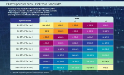 PCIe 8.0规范草案获里程碑进展:256GT/s速率开启1TB/s带宽时代

 寒武纪紧急辟谣背后:AI芯片龙头的真实现状与投资陷阱
 英伟达50亿入股英特尔:芯片巨头联手剑指AMD,行业格局生变
 闪迪预警:NAND闪存供应短缺将持续至2026年
工作时间:9:00-21:00
CEO邮箱:ceo@jiepei.com
投诉邮箱:tousu@jiepei.com


 浙公网安备 33010502006866号 浙ICP备10014259号-119
营业执照ICP证
浙公网安备 33010502006866号 浙ICP备10014259号-119
营业执照ICP证


