DP83826E, DP83826I
ZHCSKM7F –DECEMBER 2019 –REVISED NOVEMBER 2022
www.ti.com.cn
表6-1. Pin Functions (ENHANCED Mode) (continued)
PIN
TYPE (1)
DESCRIPTION
NAME
NO
Power down (default), interrupt: The default function of this pin is power down. Register
access is required to configure this pin as an interrupt. In power down function, an active low
signal on this pin places the device in power down mode. When this pin is configured as an
interrupt pin, this pin is asserted low when an interrupt condition occurs. The pin has an open-
drain output with a weak internal pullup resistor (9.5 kΩ). Some applications may require an
external PU resistor.
Reset: I, PU
Active: I, PU
PWRDN/INT
21
Reset: I, PD
Active: O
Strap5
MII transmit clock: MII transmit clock provides a 25-MHz reference clock for 100-Mbps speed
and a 2.5-MHz reference clock for 10-Mbps speed. Note that in MII mode, this clock has
constant phase referenced to the input clock. Unused in RMII Mode.
TX_CLK
TX_EN
22
23
Transmit enable: TX_EN is presented on the rising edge of the TX_CLK. TX_EN indicates the
presence of valid data inputs on TX_D[3:0] in MII mode and on TX_D[1:0] in RMII mode.
TX_EN is an active high signal.
Reset: I, PD
Active: I, PD
Reset: I, PD
Active: I, PD
TX_D0
TX_D1
TX_D2
TX_D3
24
25
26
27
Transmit data:
Reset: I, PD
Active: I, PD
In MII mode, the transmit data nibble received from the MAC is synchronous to the rising
edge of TX_CLK.
Reset: I, PD
Active: I, PD
In RMII mode, TX_D[1:0] received from the MAC is synchronous to the rising edge of the
reference clock.
Reset: I, PD
Active: I, PD
Collision Detect (default): In MII mode when the pin is acting as Collision Detect (COL), this
pin is always LOW in Full Duplex mode. In Half Duplex mode, COL is asserted HIGH only
when both transmit and receive media are non-idle. This pin can also be configured as a
second additional LED driver (LED2), the MII TX_ER signal or general purpose I/O (GPIO)
through register configurations.
Reset: I, PD
Active: O
Strap4
COL/LED2/
TX_ER GPIO
28
In RMII mode, this pin acts as LED2 by default.
Carrier sense (default):
In MII mode this pin is asserted high when the receive or transmit medium is non-idle. Carrier
Reset: I, PD
Active: O
Strap3
sense and receive data valid. This pin can be configured as third LED (LED3) through register
configuration.
CRS/LED3
LED0
29
30
In RMII mode, it is configured as LED3 by default.
LED0: This LED indicates transmit and receive activity in addition to the status of the Link.
The LED is ON when link is good. The LED blinks when the transmitter or receiver is active.
LED polarity is auto-detected (Active Low/ Active High) based on external pull-up or pull-down
on the pin.
Reset: I, PD
Active: O
Strap2
This pin provides 25-MHz reference clock from XI as default to clock. The output is not
affected by Resets allowing Application to reset PHY without impacting other system getting
impacted. The output clock switches off only by Deep Power Down.
Reset: I, PU
Active: O
Strap1
The pin can be configured to act as LED1 using strap or register configuration. The strap only
latches on power-up and not on pin reset. The LED is ON when link is 100 M. LED remains
OFF if Link is 10 M or no Link.
CLKOUT/
LED1
31
32
LED polarity is auto-detected (Active Low/ Active High) based on external pull-up or pull-down
on the pin.
Reset low: RST_N pin is an active low reset input. Asserting this pin low for at least 25 μs
forces a reset process to occur. Initiation of reset causes strap pins to be re-scanned and
resets all the internal registers of the PHY to default value.
Reset: I, PU
Active: I, PU
RST_N
(1) I = Input, O = Output, I/O = Input/Ouput, A = Analog, PU or PD = Internal pullup or pulldown: Hardware bootstrap configuration
Copyright © 2022 Texas Instruments Incorporated
Submit Document Feedback
7
Product Folder Links: DP83826E DP83826I


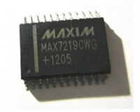
 MAX7219驱动8段数码管详解及数据手册关键信息

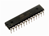
 ATMEGA328P技术资料深入分析

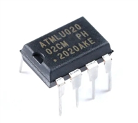
 AT24C02芯片手册管脚信息、参数分析、应用领域详解

 AT24C256芯片手册参数分析、引脚说明、读写程序示例
