DP83826E, DP83826I
ZHCSKM7F –DECEMBER 2019 –REVISED NOVEMBER 2022
www.ti.com.cn
表6-1. Pin Functions (ENHANCED Mode)
PIN
TYPE (1)
DESCRIPTION
NAME
NO
This pin selects the DP83826 operating mode: BASIC mode or ENHANCED mode. For
ENHANCED mode, this pin shall be left NC or pulled-up with a resistor to VDDIO. For BASIC
mode, this pin shall be shorted to GND.
Reset: I, PU
Active: I, PU
ModeSelect
1
CEXT
2
3
A
External capacitor: Connect the CEXT pin through a 2-nF capacitor to GND.
Input analog supply: 3V3. For decoupling capacitor requirements, refer to Power Supply
Recommendations section of data sheet.
VDDA3V3
Power
RD_M
RD_P
TD_M
TD_P
4
5
6
7
A
A
A
A
Differential receive input (physical media dependent: PMD): These differential inputs are
automatically configured to accept either 10BASE-Te, 100BASE-TX specific signaling mode.
Differential transmit output (PMD): These differential outputs are configured to either
10BASE-Te or 100BASE-TX signaling mode based on configuration chosen for PHY.
Crystal output: Reference clock output. XO pin is used for crystal only. Leave this pin floating
when a CMOS-level oscillator is connected to XI.
XO
8
A
Crystal or oscillator input clock:
MII mode, RMII master mode: 25-MHz ±50 ppm-tolerance crystal or oscillator clock.
XI/50MHzIn
9
A
A
RMII slave mode: 50-MHz ±50 ppm-tolerance CMOS-level oscillator clock.
RBIAS
MDIO
10
11
RBIAS ( Bias resistor) value 6.49 kΩwith 1% precision connected to ground.
Management data I/O: Bi-directional management data signal that may be sourced by the
management station or the PHY. This pin has internal pullup resistor of 10 kΩ. An external
pullup resistor can be added if needed.
Reset: I, PU
Active: I/O, PU
Management data clock: Synchronous clock to the MDIO serial management input/output
data. This clock may be asynchronous to the MAC transmit and receive clocks. The
maximum clock rate is 25 MHz. There is no minimum clock rate.
Reset: I, PD
Active: I, PD
MDC
12
13
14
Reset: I, PD
Active: O
Strap7
RX_D3
Reset: I, PD
Active: O
Strap8
RX_D2
RX_D1
Receive data: Symbols received on the cable are decoded and presented on these pins
synchronous to the rising edge of RX_CLK. They contain valid data when RX_DV is asserted.
A nibble RX_D[3:0] is received in MII mode. 2-bits RX_D[1:0] is received in RMII mode.
Reset: I, PD
Active: O
Strap9
15
Reset: I, PU
Active: O
Strap0
RX_D0
VDDIO
16
17
I/O supply voltage: 3.3 V/1.8 V. For decoupling capacitor requirements, refer to Power Supply
Decoupling Recommendations section of data sheet.
Power
Receive data valid: This pin indicates valid data is present on the RX_D[3:0] for MII mode and
on RX_D[1:0] in RMII mode. In MII mode, this pin acts as RX_DV. In RMII mode, this pin acts
as CRS_DV and combines the RMII Carrier and Receive Data Valid indications. This pin can
be configured to RX_DV in RMII mode to enable RMII Repeater Mode.
Reset: I, PD
Active: O
Strap10
RX_DV/
CRS_DV
18
19
MII receive clock: MII Receive Clock provides a 25-MHz reference clock for 100-Mbps speed
and a 2.5-MHz reference clock for 10-Mbps speed, which is derived from the received data
stream.
In RMII Master mode, this provides 50-MHz reference clock. In RMII Slave mode, this pin is
not used and remains Input, pulldown.
RX_CLK/
50MHz_RMII
Reset: I, PD
Active: O
Receive error: This pin indicates that an error symbol has been detected within a received
packet in both MII and RMII mode.
In MII mode, RX_ER is asserted high synchronously to the rising edge of RX_CLK.
In RMII mode, RX_ER is asserted high synchronously to the rising edge of the reference
clock. RX_ER is asserted high for every reception error, including errors during Idle.
This strap only latches on power-up and not on pin reset.
Reset: I, PD
Active: O
Strap6
RX_ER
20
Copyright © 2022 Texas Instruments Incorporated
6
Submit Document Feedback
Product Folder Links: DP83826E DP83826I


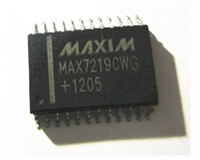
 MAX7219驱动8段数码管详解及数据手册关键信息

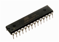
 ATMEGA328P技术资料深入分析

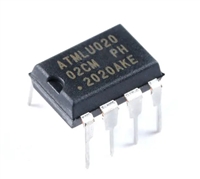
 AT24C02芯片手册管脚信息、参数分析、应用领域详解

 AT24C256芯片手册参数分析、引脚说明、读写程序示例
