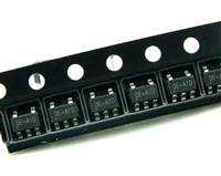
SM560
Absolute Maximum Ratings[1]
Supply Voltage (VDD):.................................... –0.5V to +6.0V
DC Input Voltage:..................................–0.5V to VDD + 0.5V
Junction Temperature .................................–40°C to +140°C
Operating Temperature:...................................... 0°C to 70°C
Storage Temperature.................................. –65°C to +150°C
Static Discharge Voltage (ESD).......................... 2,000V-Min.
Table 2. DC Electrical Characteristics: VDD = 3.3V, Temp. = 25°C and CL (Pin 4) = 15 pF, unless otherwise noted
Parameter
VDD
Description
Power Supply Range
Input High Voltage
Input Middle Voltage
Input Low Voltage
Output High Voltage
Output High Voltage
Output Low Voltage
Output Low Voltage
Input Capacitance
Input Capacitance
Input Capacitance
Power Supply Current
Power Supply Current
Conditions
Min.
2.97
Typ.
3.3
Max.
3.63
VDD
Unit
V
±10%
VINH
VINM
VINL
VOH1
VOH2
VOL1
VOL2
Cin1
Cin2
Cin2
IDD1
S0 and S1 only
S0 and S1 only
S0 and S1 only
IOH = 6 mA
0.85VDD
VDD
V
0.40VDD 0.50VDD 0.60VDD
V
0.0
2.4
2.0
0.0
0.15VDD
V
V
IOH = 20 mA
V
IOH = 6 mA
0.4
1.2
5
V
IOH = 20 mA
V
Xin/CLK (Pin 1)
Xout (Pin 8)
3
6
3
4
8
pF
pF
pF
mA
mA
10
5
S0, S1, SSCC (Pins 7,6,5)
FIN = 40 MHz
FIN = 65 MHz
4
30
35
40
45
IDD2
Table 3. Electrical Timing Characteristics: VDD = 3.3V, T = 25°C and CL = 15 pF, unless otherwise noted
Parameter
ICLKFR
Trise
Description
Input Clock Frequency Range
Clock Rise Time (Pin 4)
Clock Fall Time (Pin 4)
Input Clock Duty Cycle
Output Clock Duty Cycle
Cycle-to-Cycle Jitter
Conditions
VDD = 3.30V
Min.
25
1.2
1.2
20
45
-
Typ.
Max.
108
1.6
1.6
80
Unit
MHz
ns
SSCLK1 @ 0.4 – 2.4V
SSCLK1 @ 0.4 – 2.4V
XIN/CLK (Pin 1)
1.4
1.4
50
Tfall
ns
DTYin
%
DTYout
JCC
SSCLK1 (Pin 4)
50
55
%
Fin = 25 – 108 MHz
125
175
ps
electronic equipment by the amount of peak energy radiated
from the equipment. By reducing the peak energy at the funda-
mental and harmonic frequencies, the equipment under test is
able to satisfy agency requirements for EMI. Conventional
methods of reducing EMI have been to use shielding, filtering,
multi-layer PCBs, etc. The SM560 uses the approach of
reducing the peak energy in the clock by increasing the clock
bandwidth, and lowering the Q.
SSCG Theory of Operation
The SM560 is a PLL-type clock generator using a proprietary
Cypress design. By precisely controlling the bandwidth of the
output clock, the SM560 becomes a Low EMI clock generator.
The theory and detailed operation of the SM560 will be
discussed in the following sections.
EMI
SSCG
All digital clocks generate unwanted energy in their harmonics.
Conventional digital clocks are square waves with a duty cycle
that is very close to 50%. Because of this 50/50-duty cycle,
digital clocks generate most of their harmonic energy in the
odd harmonics, i.e.; third, fifth, seventh, etc. It is possible to
reduce the amount of energy contained in the fundamental
and odd harmonics by increasing the bandwidth of the funda-
mental clock frequency. Conventional digital clocks have a
very high Q factor, which means that all of the energy at that
frequency is concentrated in a very narrow bandwidth, conse-
SSCG uses a patented technology of modulating the clock
over a very narrow bandwidth and controlled rate of change,
both peak and cycle to cycle. The SM560 takes a narrow band
digital reference clock in the range of 25–108 MHz and
produces a clock that sweeps between a controlled start and
stop frequency and precise rate of change. To understand
what happens to a clock when SSCG is applied, consider a
65-MHz clock with a 50% duty cycle. From a 65-MHz clock we
know the following:
quently, higher energy peaks. Regulatory agencies test
Note:
1. Single Power Supply: The Voltage on any input or I/O pin cannot exceed the power pin during power up.
Document #: 38-07020 Rev. *E
Page 4 of 8
[+] Feedback


 一文带你解读74HC244资料手册:特性、应用场景、封装方式、引脚配置说明、电气参数、推荐替代型号

 AD623资料手册解读:特性、应用、封装、引脚功能及电气参数

 RT9193资料手册解读:RT9193引脚功能、电气参数、替换型号推荐

 VIPER22A的资料手册解读、引脚参数说明、代换型号推荐
