
| 是否无铅: | 不含铅 | 是否Rohs认证: | 符合 |
| 生命周期: | Active | 包装说明: | LCC10,.27SQ,66 |
| Reach Compliance Code: | unknown | 风险等级: | 5.72 |
| Is Samacsys: | N | 特性阻抗: | 50 Ω |
| 构造: | COMPONENT | 增益: | 20 dB |
| 最大输入功率 (CW): | 8 dBm | JESD-609代码: | e4 |
| 安装特点: | SURFACE MOUNT | 功能数量: | 1 |
| 端子数量: | 10 | 最大工作频率: | 925 MHz |
| 最小工作频率: | 887 MHz | 最高工作温度: | 90 °C |
| 最低工作温度: | -30 °C | 封装主体材料: | CERAMIC |
| 封装等效代码: | LCC10,.27SQ,66 | 电源: | 1/4.2 V |
| 射频/微波设备类型: | NARROW BAND LOW POWER | 子类别: | RF/Microwave Amplifiers |
| 最大压摆率: | 420 mA | 表面贴装: | YES |
| 端子面层: | Gold (Au) | 最大电压驻波比: | 2 |
| Base Number Matches: | 1 |
| 型号 | 品牌 | 获取价格 | 描述 | 数据表 |
| CXG1158K | SONY |
获取价格 |
Power Amplifier Module for JCDMA |

|
| CXG1166AER | SONY |
获取价格 |
High Power 3 x 5 Antenna Switch MMIC with Integrated Control Logic |
|
| CXG1166ER | SONY |
获取价格 |
High Power 3 × 5 Antenna Switch MMIC with Int |
|
| CXG1171UR | SONY |
获取价格 |
Diversity Switch, 1920MHz Min, 2170MHz Max, 1 Func, 1.15dB Insertion Loss-Max, GAAS, 2.70 |
|
| CXG1172UR | SONY |
获取价格 |
JPHEMT High Power DPDT Switch with Logic Control |
|
| CXG1173UR | SONY |
获取价格 |
High Power SPDT Switch with Logic Control |
|
| CXG1174UR | SONY |
获取价格 |
High Power SP3T Switch with Logic Control |
|
| CXG1175UR | SONY |
获取价格 |
Diversity Switch, 830MHz Min, 2170MHz Max, 1 Func, 0.8dB Insertion Loss-Max, GAAS, PLASTIC |
|
| CXG1176UR | SONY |
获取价格 |
High Power DPDT Switch with Logic Control |
|
| CXG1177UR | SONY |
获取价格 |
Diversity Switch, 830MHz Min, 2170MHz Max, 2 Func, 0.75dB Insertion Loss-Max, GAAS, PLASTI |
|
 英伟达Rubin GPU量产或延后:性能飞跃背后的时间博弈

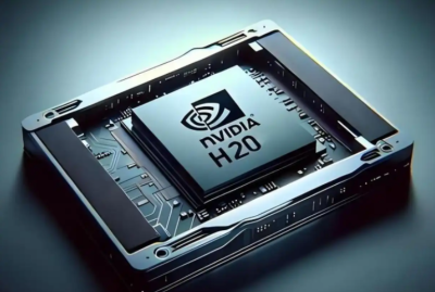 外媒爆料:美国秘密在AI芯片中植入追踪器监控中国供应链
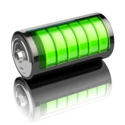 中国科学家突破锂电池技术瓶颈:能量密度提升3倍将改写行业格局
 西北工业大学突破极寒技术:抗冻机器人轻松应对-50°C极端环境
工作时间:9:00-21:00
CEO邮箱:ceo@jiepei.com
投诉邮箱:tousu@jiepei.com


 浙公网安备 33010502006866号 浙ICP备10014259号-119
营业执照ICP证
浙公网安备 33010502006866号 浙ICP备10014259号-119
营业执照ICP证


