ADVANCE
S27KL0641, S27KS0641
Table 5.2 ID Register 0 Bit Assignments (Continued)
Bits
Function
Settings (Binary)
0000 - One column address bit
...
1111 - Sixteen column address bits
7-4
3-0
Column Address Bit Count
0000 - Reserved
0001 - Spansion
Manufacturer
0010 to 1111 - Reserved
Table 5.3 ID Register 1 Bit Assignments
Bits
Function
Settings (Binary)
15-4
Reserved
0000_0000_0000b (default)
0000 - HyperRAM
0001 to 1111 - Reserved
3-0
Device Type
5.1.1
Density and Row Boundaries
The DRAM array size (density) of the device can be determined from the total number of system address bits used for the row and
column addresses as indicated by the Row Address Bit Count and Column Address Bit Count fields in the ID0 register. For example:
a 64 Mbit HyperRAM has 9 column address bits and 13 row address bits for a total of 22 word address bits = 222 = 4 Mwords =
8 Mbytes. The 9 column address bits indicate that each row holds 29 = 512 words = 1 kbytes. The row address bit count indicates
there are 8196 rows to be refreshed within each array refresh interval. The row count is used in calculating the refresh interval.
5.2
Register Space Access
Register default values are loaded upon power-up or hardware reset. The registers can be altered at any time while the device is in
the standby state.
Loading a register is accomplished with a single 16-bit word write transaction as shown in Figure 5.1. CA[47] is zero to indicate a
write transaction, CA[46] is a one to indicate a register space write, CA[45] is a one to indicate a linear write, lower order bits in the
CA field indicate the register address.
Figure 5.1 Loading a Register
CS#
CK,CK#
Memory drives RWDS with Refresh Indication
RWDS
47:40
39:32
31:24
23:16
15:8
7:0
15:8
7:0
DQ[7:0]
Command-Address
RD
Host drives DQ[7:0] with Command-Address and Register Data
Notes:
1. The host must not drive RWDS during a write to register space.
2. The RWDS signal is driven by the memory during the Command-Address period based on whether the memory array is being
refreshed. This refresh indication does not affect the writing of register data. RWDS is driven immediately after CS# goes low,
before CA[47:46] are received to indicate that the transaction is a write to register space, for which the RWDS refresh indication is
not relevant.
3. The register value is always provided immediately after the CA value and is not delayed by a refresh latency.
4. The the RWDS signal returns to high impedance after the Command-Address period. Register data is never masked. Both data
bytes of the register data are loaded into the selected register.
Document Number: 001-97964 Rev. *E
Page 8 of 29


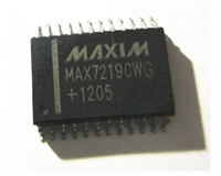
 MAX7219驱动8段数码管详解及数据手册关键信息

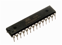
 ATMEGA328P技术资料深入分析

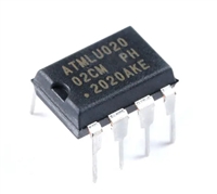
 AT24C02芯片手册管脚信息、参数分析、应用领域详解

 AT24C256芯片手册参数分析、引脚说明、读写程序示例
