
 5秒后页面跳转

| 型号 | 品牌 | 获取价格 | 描述 | 数据表 |
| 5962-9458501HTA | ETC |
获取价格 |
x32 EEPROM Module |

|
| 5962-9458501HTC | ETC |
获取价格 |
x32 EEPROM Module |
|
| 5962-9458501HUA | ETC |
获取价格 |
x32 EEPROM Module |
|
| 5962-9458501HUC | ETC |
获取价格 |
x32 EEPROM Module |
|
| 5962-9458501HXA | ETC |
获取价格 |
x32 EEPROM Module |
|
| 5962-9458501HXC | ETC |
获取价格 |
x32 EEPROM Module |
|
| 5962-9458501HYA | ETC |
获取价格 |
x32 EEPROM Module |
|
| 5962-9458501HYC | ETC |
获取价格 |
x32 EEPROM Module |
|
| 5962-9458501HYX | WEDC |
获取价格 |
EEPROM Module, 128KX32, 300ns, Parallel, CMOS, HIP-66 |
|
| 5962-9458502H4A | MICROSS |
获取价格 |
EEPROM, 128KX32, 250ns, Parallel, CMOS, CPGA66, PGA-66 |
|
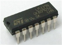 LM339N参数手册 :四路电压比较器的深度解读

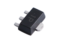 MMBT2222A资料手册:特性、应用、电气参数及替换型号推荐
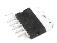 解读TDA7265手册资料:引脚说明 、电气参数及替换型号推荐
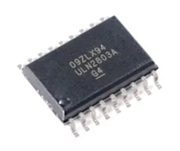 深入解读ULN2803A资料手册:引脚功能、电气参数、特性
工作时间:9:00-21:00
CEO邮箱:ceo@jiepei.com
投诉邮箱:tousu@jiepei.com


 浙公网安备 33010502006866号 浙ICP备10014259号-119
营业执照ICP证
浙公网安备 33010502006866号 浙ICP备10014259号-119
营业执照ICP证


