MITSUBISHI RF POWER MODULE
ELECTROSTATIC SENSITIVE DEVICE
OBSERVE HANDLING PRECAUTIONS
RoHS COMPLIANCE RA08H1317M
PRECAUTIONS, RECOMMENDATIONS, and APPLICATION INFORMATION:
Construction:
This module consists of an alumina substrate soldered onto a copper flange. For mechanical protection, a plastic
cap is attached with silicone. The MOSFET transistor chips are die bonded onto metal, wire bonded to the
substrate, and coated with resin. Lines on the substrate (eventually inductors), chip capacitors, and resistors form
the bias and matching circuits. Wire leads soldered onto the alumina substrate provide the DC and RF connection.
Following conditions must be avoided:
a) Bending forces on the alumina substrate (for example, by driving screws or from fast thermal changes)
b) Mechanical stress on the wire leads (for example, by first soldering then driving screws or by thermal expansion)
c) Defluxing solvents reacting with the resin coating on the MOSFET chips (for example, Trichlorethylene)
d) Frequent on/off switching that causes thermal expansion of the resin
e) ESD, surge, overvoltage in combination with load VSWR, and oscillation
ESD:
This MOSFET module is sensitive to ESD voltages down to 1000V. Appropriate ESD precautions are required.
Mounting:
Heat sink flatness must be less than 50 µm (a heat sink that is not flat or particles between module and heat sink
may cause the ceramic substrate in the module to crack by bending forces, either immediately when driving screws
or later when thermal expansion forces are added).
A thermal compound between module and heat sink is recommended for low thermal contact resistance and to
reduce the bending stress on the ceramic substrate caused by the temperature difference to the heat sink.
The module must first be screwed to the heat sink, then the leads can be soldered to the printed circuit board.
M3 screws are recommended with a tightening torque of 0.4 to 0.6 Nm.
Soldering and Defluxing:
This module is designed for manual soldering.
The lead (terminal) must be soldered after the module is screwed onto the heat sink.
The temperature of the lead (terminal) soldering should be lower than 350°C and shorter than 3 second.
Ethyl Alcohol is recommend for removing flux. Trichloroethylene solvents must not be used (they may cause
bubbles in the coating of the transistor chips which can lift off the bond wires).
Thermal Design of the Heat Sink:
At Pout=8W, VDD=12.5V and Pin=20mW each stage transistor operating conditions are:
Pin
(W)
Pout
(W)
Rth(ch-case)
(°C/W)
IDD @ ηT=40%
VDD
(V)
Stage
(A)
1st
2nd
0.02
1.5
1.5
8.0
4.0
2.4
0.3
12.5
1.32
The channel temperatures of each stage transistor Tch = Tcase + (VDD x IDD - Pout + Pin) x Rth(ch-case) are:
Tch1 = Tcase + (12.5V x 0.3A – 1.5W + 0.02W) x 4.0°C/W
Tch2 = Tcase + (12.5V x 1.32A – 8.0W + 1.5W) x 2.4°C/W
= Tcase + 9.1 °C
= Tcase + 24.0 °C
For long-term reliability, it is best to keep the module case temperature (Tcase) below 90°C. For an ambient
temperature Tair=60°C and Pout=8W, the required thermal resistance Rth (case-air) = ( Tcase - Tair) / ( (Pout / ηT ) - Pout
+ Pin ) of the heat sink, including the contact resistance, is:
Rth(case-air) = (90°C - 60°C) / (8W/40% – 8W + 0.02W) = 2.50 °C/W
When mounting the module with the thermal resistance of 2.50 °C/W, the channel temperature of each stage
transistor is:
Tch1 = Tair + 39.1 °C
Tch2 = Tair + 54.0 °C
The 175°C maximum rating for the channel temperature ensures application under derated conditions.
RA08H1317M
24 Jan 2006
MITSUBISHI ELECTRIC
7/8


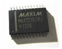
 MAX7219驱动8段数码管详解及数据手册关键信息

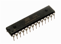
 ATMEGA328P技术资料深入分析

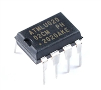
 AT24C02芯片手册管脚信息、参数分析、应用领域详解

 AT24C256芯片手册参数分析、引脚说明、读写程序示例
