32GB (x72, ECC, DR) 288-Pin DDR4 RDIMM
Pin Descriptions
Table 5: Pin Descriptions (Continued)
Symbol
Type
Description
ODTx
Input
On-die termination: ODT (registered HIGH) enables termination resistance internal to the
DDR4 SDRAM. When enabled, ODT (RTT) is applied only to each DQ, DQS_t, DQS_c, DM_n/
DBI_n/TDQS_t, and TDQS_c signal for x4 and x8 configurations (when the TDQS function is ena-
bled via the mode register). For the x16 configuration, RTT is applied to each DQ, DQSU_t,
DQSU_c, DQSL_t, DQSL_c, UDM_n, and LDM_n signal. The ODT pin will be ignored if the mode
registers are programmed to disable RTT
.
PARITY
Input
Input
Parity for command and address: This function can be enabled or disabled via the mode
register. When enabled in MR5, the DRAM calculates parity with ACT_n, RAS_n/A16, CAS_n/A15,
WE_n/A14, BG[1:0], BA[1:0], A[16:0]. Input parity should be maintained at the rising edge of the
clock and at the same time as command and address with CS_n LOW.
RAS_n/A16
CAS_n/A15
WE_n/A14
Command inputs: RAS_n/A16, CAS_n/A15, and WE_n/A14 (along with CS_n) define the com-
mand and/or address being entered and have multiple functions. For example, for activation
with ACT_n LOW, these are addresses like A16, A15, and A14, but for a non-activation com-
mand with ACT_n HIGH, these are command pins for READ, WRITE, and other commands de-
fined in Command Truth Table.
RESET_n
SAx
CMOS Input Active LOW asynchronous reset: Reset is active when RESET_n is LOW and inactive when RE-
SET_n is HIGH. RESET_n must be HIGH during normal operation.
Serial address inputs: Used to configure the temperature sensor/SPD EEPROM address range
Input
on the I2C bus.
Serial clock for temperature sensor/SPD EEPROM: Used to synchronize communication to
SCL
Input
and from the temperature sensor/SPD EEPROM on the I2C bus.
DQx, CBx
I/O
Data input/output and check bit input/output: Bidirectional data bus. DQ represents
DQ[3:0], DQ[7:0], and DQ[15:0] for the x4, x8, and x16 configurations, respectively. If cyclic re-
dundancy checksum (CRC) is enabled via the mode register, the CRC code is added at the end of
the data burst. Any one or all of DQ0, DQ1, DQ2, or DQ3 may be used for monitoring of inter-
nal VREF level during test via mode register setting MR[4] A[4] = HIGH; training times change
when enabled.
DM_n/DBI_n/
TDQS_t (DMU_n,
DBIU_n), (DML_n/
DBIl_n)
I/O
Input data mask and data bus inversion: DM_n is an input mask signal for write data. Input
data is masked when DM_n is sampled LOW coincident with that input data during a write ac-
cess. DM_n is sampled on both edges of DQS. DM is multiplexed with the DBI function by the
mode register A10, A11, and A12 settings in MR5. For a x8 device, the function of DM or TDQS
is enabled by the mode register A11 setting in MR1. DBI_n is an input/output identifying
whether to store/output the true or inverted data. If DBI_n is LOW, the data will be stored/
output after inversion inside the DDR4 device and not inverted if DBI_n is HIGH. TDQS is only
supported in x8 SDRAM configurations (TDQS is not valid for UDIMMs).
SDA
I/O
I/O
Serial Data: Bidirectional signal used to transfer data in or out of the EEPROM or EEPROM/TS
combo device.
DQS_t
DQS_c
DQSU_t
DQSU_c
DQSL_t
DQSL_c
Data strobe: Output with read data, input with write data. Edge-aligned with read data, cen-
tered-aligned with write data. For x16 configurations, DQSL corresponds to the data on
DQ[7:0], and DQSU corresponds to the data on DQ[15:8]. For the x4 and x8 configurations, DQS
corresponds to the data on DQ[3:0] and DQ[7:0], respectively. DDR4 SDRAM supports a differen-
tial data strobe only and does not support a single-ended data strobe.
ALERT_n
Output
Output
Alert output: Possesses functions such as CRC error flag and command and address parity error
flag as output signal. If a CRC error occurs, ALERT_n goes LOW for the period time interval and
returns HIGH. If an error occurs during a command address parity check, ALERT_n goes LOW un-
til the on-going DRAM internal recovery transaction is complete. During connectivity test mode,
this pin functions as an input. Use of this signal is system-dependent. If not connected as signal,
ALERT_n pin must be connected to VDD on DIMMs.
EVENT_n
Temperature event: The EVENT_n pin is asserted by the temperature sensor when critical tem-
perature thresholds have been exceeded. This pin has no function (NF) on modules without
temperature sensors.
PDF: 09005aef85e8fa27
asf36c4gx72pz.pdf - Rev. F 8/16 EN
Micron Technology, Inc. reserves the right to change products or specifications without notice.
6
© 2014 Micron Technology, Inc. All rights reserved.


 压敏电阻器在直流电路中的过压保护应用探讨

 电感耐压值及其与电感大小的关系

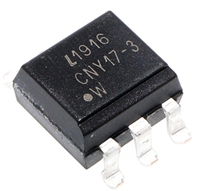
 CNY17F光耦合器:特性、应用、封装、引脚功能及替换型号解析

 DS1307资料解析:特性、引脚说明、替代推荐
