
 5秒后页面跳转

| 是否无铅: | 不含铅 | 是否Rohs认证: | 符合 |
| 生命周期: | Active | 包装说明: | LQFP-48 |
| Reach Compliance Code: | compliant | 风险等级: | 5.7 |
| Base Number Matches: | 1 |
| 型号 | 品牌 | 获取价格 | 描述 | 数据表 |
| MC33910 | FREESCALE |
获取价格 |
LIN System Basis Chip with High Side Drivers |

|
| MC33910BAC | FREESCALE |
获取价格 |
LIN System Basis Chip with 2x60mA High Side Drivers |
|
| MC33910BAC | NXP |
获取价格 |
System Basis Chip, LIN, 1x 5.0V/60mA LDOs, High-Side Drivers, QFP 32 |
|
| MC33910BACR2 | FREESCALE |
获取价格 |
LIN System Basis Chip with 2x60mA High Side Drivers |
|
| MC33910G5AC | FREESCALE |
获取价格 |
LIN System Basis Chip with High |
|
| MC33910G5AC | ROCHESTER |
获取价格 |
0.11A BUF OR INV BASED PRPHL DRVR, PQFP32, 7 X 7 MM, 1.40 MM HEIGHT, 0.80 MM PITCH, ROHS C |
|
| MC33910G5AC | NXP |
获取价格 |
System Basis Chip, LIN, 1x 5.0V/60mA LDOs, High-Side Drivers, Enhanced EMC, QFP 32 |
|
| MC33910G5AC/R2 | FREESCALE |
获取价格 |
LIN System Basis Chip with High Side Drivers |
|
| MC33911 | FREESCALE |
获取价格 |
LIN System Basis Chip with DC Motor Pre-driver |
|
| MC33911_10 | FREESCALE |
获取价格 |
LIN System Basis Chip with DC Motor Pre-driver |
|
 US1M数据手册解读:产品特性、替换型号推荐

 解析BAV99LT1G手册:参数分析、替换型号推荐
 解读BSS138PW数据手册:产品特性、电气参数及替换型号推荐
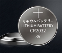 CR2032资料手册解读:参数分析、替换型号推荐
工作时间:9:00-21:00
CEO邮箱:ceo@jiepei.com
投诉邮箱:tousu@jiepei.com


 浙公网安备 33010502006866号 浙ICP备10014259号-119
营业执照ICP证
浙公网安备 33010502006866号 浙ICP备10014259号-119
营业执照ICP证


