
 5秒后页面跳转

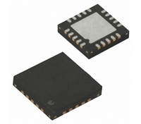
| 生命周期: | Obsolete | 包装说明: | LFBGA, |
| Reach Compliance Code: | unknown | 风险等级: | 5.84 |
| 访问模式: | FOUR BANK PAGE BURST | 最长访问时间: | 5.5 ns |
| 其他特性: | AUTO/SELF REFRESH | JESD-30 代码: | R-PBGA-B90 |
| 长度: | 13 mm | 内存密度: | 134217728 bit |
| 内存集成电路类型: | SYNCHRONOUS DRAM | 内存宽度: | 32 |
| 功能数量: | 1 | 端口数量: | 1 |
| 端子数量: | 90 | 字数: | 4194304 words |
| 字数代码: | 4000000 | 工作模式: | SYNCHRONOUS |
| 最高工作温度: | 70 °C | 最低工作温度: | |
| 组织: | 4MX32 | 封装主体材料: | PLASTIC/EPOXY |
| 封装代码: | LFBGA | 封装形状: | RECTANGULAR |
| 封装形式: | GRID ARRAY, LOW PROFILE, FINE PITCH | 座面最大高度: | 1.4 mm |
| 自我刷新: | YES | 最大供电电压 (Vsup): | 3.6 V |
| 最小供电电压 (Vsup): | 3 V | 标称供电电压 (Vsup): | 3.3 V |
| 表面贴装: | YES | 技术: | CMOS |
| 温度等级: | COMMERCIAL | 端子形式: | BALL |
| 端子节距: | 0.8 mm | 端子位置: | BOTTOM |
| 宽度: | 8 mm |
| 型号 | 品牌 | 获取价格 | 描述 | 数据表 |
| M12L128324A-6BIG | ESMT |
获取价格 |
1M x 32 Bit x 4 Banks Synchronous DRAM |

|
| M12L128324A-6BIG2E | ESMT |
获取价格 |
Synchronous DRAM, 4MX32, 5.5ns, CMOS, PBGA90, FBGA-90 |
|
| M12L128324A-6TG | ESMT |
获取价格 |
1M x 32 Bit x 4 Banks Synchronous DRAM |
|
| M12L128324A-6TIG | ESMT |
获取价格 |
1M x 32 Bit x 4 Banks Synchronous DRAM |
|
| M12L128324A-7BG | ESMT |
获取价格 |
1M x 32 Bit x 4 Banks Synchronous DRAM |
|
| M12L128324A-7BG2E | ESMT |
获取价格 |
JEDEC standard 3.3V power supply |
|
| M12L128324A-7BIG | ESMT |
获取价格 |
1M x 32 Bit x 4 Banks Synchronous DRAM |
|
| M12L128324A-7TG | ESMT |
获取价格 |
1M x 32 Bit x 4 Banks Synchronous DRAM |
|
| M12L128324A-7TIG | ESMT |
获取价格 |
1M x 32 Bit x 4 Banks Synchronous DRAM |
|
| M12L16161A | ESMT |
获取价格 |
512K x 16Bit x 2Banks Synchronous DRAM |
|
 ATA6621N数据手册解读:产品特性、引脚图信息、电气参数

 一文AO3400引脚图、参数、产品特性
 数据手册解读:MB10S引脚说明、电气参数
 2N7002K资料解读:产品特性和型号推荐
工作时间:9:00-21:00
CEO邮箱:ceo@jiepei.com
投诉邮箱:tousu@jiepei.com


 浙公网安备 33010502006866号 浙ICP备10014259号-119
营业执照ICP证
浙公网安备 33010502006866号 浙ICP备10014259号-119
营业执照ICP证


