HY29DS322/HY29DS323
32 Megabit (4M x 8/2M x16) Super-Low Voltage,
Dual Bank, Simultaneous Read/Write, Flash Memory
KEY FEATURES
n Single Power Supply Operation
n Data# Polling and Toggle Bits
− Read, program, and erase operations
− Provide software confirmation of completion
from 1.8 to 2.2 V (2.0V ± 10%)
of program or erase operations
− Ideal for battery-powered applications
n Simultaneous Read/Write Operations
− Host system can program or erase in one
bank while simultaneously reading from any
sector in the other bank with zero latency
between read and write operations
n High Performance
n Ready/Busy# Pin
− Provides hardware confirmation of
completion of program or erase operations
n Erase Suspend
− Suspends an erase operation to allow
programming data to or reading data from
a sector in the same bank
− 100, 110 and 120 ns access time versions
n Ultra Low Power Consumption (Typical
Values)
− Erase Resume can then be invoked to
complete the suspended erasure
n Hardware Reset Pin (RESET#) Resets the
Device to Reading Array Data
n WP#/ACC Input Pin
− Automatic sleep mode current: 5 µA
− Standby mode current: 5 µA
− Read current: 5 mA (at 5 MHz)
− Program/erase current: 20 mA
n Boot-Block Sector Architecture with 71
Sectors in Two Banks for Fast In-System
Code Changes
− Write protect (WP#) function allows
hardware protection of two outermost boot
sectors, regardless of sector protect status
− Acceleration (ACC) function provides
accelerated program times
n Secured Sector: An Extra 64 Kbyte Sector
that Can Be:
n Fast Program and Erase Times
− Sector erase time: 2 sec typical
− Byte/Word program time utilizing
Acceleration function: 10 µs typical
n Space Efficient Packaging
− 48-pin TSOP and 48-ball FBGA
packages
− Factory locked and identifiable: 16 bytes
available for a secure, random factory
Electronic Serial Number
− Customer lockable: Can be read, program-
med, or erased just like other sectors
n Flexible Sector Architecture
− Sector Protection allows locking of a
sector or sectors to prevent program or
erase operations within that sector
− Temporary Sector Unprotect allows
changes in locked sectors (requires high
voltage on RESET# pin)
n Automatic Erase Algorithm Erases Any
Combination of Sectors or the Entire Chip
n Automatic Program Algorithm Writes and
Verifies Data at Specified Addresses
n Compliant with Common Flash Memory
Interface (CFI) Specification
LOGIC DIAGRAM
21
15
A[20:0]
CE#
DQ[14:0]
DQ[15]/A[-1]
WP#/ACC
RY/BY#
OE#
W E #
n Minimum 100,000 Write Cycles per Byte/
Word
n Compatible with JEDEC Standards
− Pinout and software compatible with
single-power supply Flash devices
− Superior inadvertent write protection
RESET#
BYTE#
Product Brief May 2001


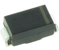
 MBRS340T3G手册解读:参数说明、产品特性及应用

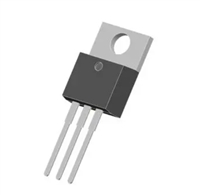
 PMOS管背靠背连接:串联还是并联?

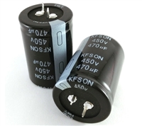
 高压电解电容的分类与选型策略

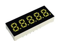
 数码管:基本概念、分类、技术发展及市场趋势
