
| 型号 | 品牌 | 获取价格 | 描述 | 数据表 |
| CXK77K36R320GB-33 | SONY |
获取价格 |
32Mb LW R-R HSTL High Speed Synchronous SRAM (1Mb x 36) |

|
| CXK77K36R320GB-4 | SONY |
获取价格 |
32Mb LW R-R HSTL High Speed Synchronous SRAM (1Mb x 36) |
|
| CXK77L18162AGB | ETC |
获取价格 |
MEMORY-UHS Synch SRAMs</A></I> 16Meg Ultra-Hi |
|
| CXK77L18162GB | ETC |
获取价格 |
MEMORY-UHS Synch SRAMs 16Meg Ultra-High-Speed Synchronous SRAM (1M x 18) (23 pages 312K Re |
|
| CXK77L18162GB-25 | SONY |
获取价格 |
DDR SRAM, 1MX18, 1.8ns, CMOS, PBGA153, 14 X 22 MM, 1.27 MM PITCH, BGA-153 |
|
| CXK77L18162GB-3 | SONY |
获取价格 |
DDR SRAM, 1MX18, 1.9ns, CMOS, PBGA153, 14 X 22 MM, 1.27 MM PITCH, BGA-153 |
|
| CXK77L18R160GB | ETC |
获取价格 |
MEMORY-UHS Synch SRAMs</A></I> 16Meg Ultra-Hi |
|
| CXK77L18R160GB-4 | SONY |
获取价格 |
Late-Write SRAM, 1MX18, 2ns, CMOS, PBGA119, 14 X 22 MM, 1.27 MM PITCH, BGA-119 |
|
| CXK77N18B160GB-3 | SONY |
获取价格 |
Late-Write SRAM, 1MX18, 1.5ns, CMOS, PBGA119, 14 X 22 MM, 1.27 MM PITCH, BGA-119 |
|
| CXK77N18B160GB-33 | SONY |
获取价格 |
Late-Write SRAM, 1MX18, 1.6ns, CMOS, PBGA119, 14 X 22 MM, 1.27 MM PITCH, BGA-119 |
|
 英伟达Rubin GPU量产或延后:性能飞跃背后的时间博弈

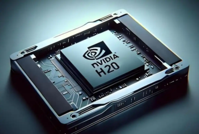 外媒爆料:美国秘密在AI芯片中植入追踪器监控中国供应链
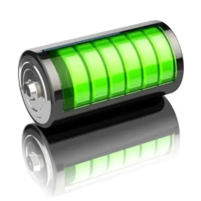 中国科学家突破锂电池技术瓶颈:能量密度提升3倍将改写行业格局
 西北工业大学突破极寒技术:抗冻机器人轻松应对-50°C极端环境
工作时间:9:00-21:00
CEO邮箱:ceo@jiepei.com
投诉邮箱:tousu@jiepei.com


 浙公网安备 33010502006866号 浙ICP备10014259号-119
营业执照ICP证
浙公网安备 33010502006866号 浙ICP备10014259号-119
营业执照ICP证


