3.16
DUAL ACCESS.BUS INTERFACE
3.21
POWER MANAGEMENT
The two ACCESS.bus (ACB) interface modules support a The Power Management Module (PMM) improves the effi-
two-wire serial interface compatible with the ACCESS.bus ciency of the device by changing the operating mode and
physical layer. It is also compatible with Intel’s System Man- power consumption to match the required level of activity.
agement Bus (SMBus) and Philips’ I2C bus. The ACB mod-
ules can be configured as a bus master or slave, and they
can maintain bidirectional communications with both multi-
high-frequency clock. All device functions are fully op-
ple master and slave devices.
The device can operate in any of four power modes:
— Active: The device operates at full speed using the
erational.
The ACCESS.bus receivers can trigger a wake-up condition
— Power Save: The device operates at reduced speed
out of the low-power modes through the Multi-Input Wake-
using the Slow Clock. The CPU and some modules
Up module.
can continue to operate at this low speed.
— Idle: The device is inactive except for the Power Man-
3.17
DUAL MULTI-FUNCTION TIMER
agement Module and Timing and Watchdog Module,
which continue to operate using the Slow Clock.
— Halt: The device is inactive but still retains its internal
state (RAM and register contents).
The two Multi-Function Timer (MFT) modules each contain
a pair of 16-bit timer/counter registers. Each timer/counter
unit can be configured to operate in any of the following
modes:
The PMM provides a mechanism to handle Bluetooth-spe-
cific power management modes, for optimizing power con-
sumption during special Bluetooth states, like Park, Page
Scan, Inquiry Scan, etc.
— Processor-Independent Pulse Width Modulation
(PWM) mode: Generates pulses of a specified width
and duty cycle and provides a general-purpose timer/
counter.
3.22
INPUT/OUTPUT PORTS
— Dual Input Capture mode: Measures the elapsed time
between occurrences of external event and provides
a general-purpose timer/counter.
— Dual Independent Timer mode: Generates system
timing signals or counts occurrences of external
events.
— Single Input Capture and Single Timer mode: Pro-
vides one external event counter and one system tim-
er.
The device has 64 software-configurable I/O pins (36 in the
FBGA-144 package), organized into four ports called Port
E, Port F, Port G, and Port H. Each pin can be configured to
operate as a general-purpose input or general-purpose out-
put. In addition, many I/O pins can be configured to operate
as inputs or outputs for on-chip peripheral modules such as
the UARTs or timers.
The I/O pin characteristics are fully programmable. Each pin
can be configured to operate as a TRI-STATE output, push-
pull output, weak pullup/pulldown input, high-speed drive, or
high-impedance input.
3.18
VERSATILE TIMER UNITS
The two Versatile Timer Unit (VTU) modules each contain
four independent timer subsystems, which operate as a
dual 8-bit PWM configuration, a single 16-bit PWM timer, or
a 16-bit counter with two input capture channels. Each of
the timer subsystems offer an 8-bit clock prescaler to ac-
commodate a wide range of frequencies.
3.23
CLOCK AND RESET MODULE
The Clock and Reset module generates a 12-MHz Main
Clock from an external crystal network or external clock in-
put. Main Clock may be used as a reference clock for two
PLL-based clock multipliers available for generating higher-
speed clocks.
3.19
TIMING AND WATCHDOG MODULE
The Timing and Watchdog Module (TWM) contains a Real-
Time timer and a Watchdog unit. The Real-Time Clock Tim-
ing function can be used to generate periodic real-time
based system interrupts. The timer output is one of 16 in-
puts to the Multi-Input Wake-Up module which can be used
to exit from a low-power mode. The Watchdog unit is de-
signed to detect the application program getting stuck in an
infinite loop resulting in loss of program control or “runaway”
programs. When the watchdog triggers, it resets the device.
The TWM is clocked by the low-speed Slow Clock.
Most modules operate from clocks derived from Main Clock
or a PLL clock. Modules on the CPU core AHB bus operate
from HCLK Clock, while modules on the peripheral APB
buses operate from PCLK Clock. PCLK Clock is generated
by dividing HCLK Clock by 1, 2, or 4. Some peripheral mod-
ules may use one of several auxiliary clocks, which also are
derived from Main Clock or a PLL clock using 12-bit pro-
grammable prescalers.
In Power-Save mode, HCLK Clock is driven by Slow Clock,
which is typically a 32.768 kHz signal generated from an ex-
ternal clock network or a prescaled Main Clock may be used
to eliminate the 32.768 kHz crystal network, for the most
cost-sensitive applications. In the most power-sensitive ap-
plications, operation from an external 32.768 kHz crystal
network allows the high-frequency oscillator and PLLs to be
shut down.
3.20
MULTI-INPUT WAKE-UP
The Multi-Input Wake-Up (MIWU) feature is used to return
(wake-up) the device from low-power modes to the active
mode. The 64-channel MIWU unit receives wake-up signals
from various internal and external sources. In addition to the
wake-up function, the MIWU unit can generate up to eight
interrupt requests. Each MIWU channel can be individually
programmed to activate one of the interrupt requests.
5
www.national.com


 MAX6675资料手册参数详解、引脚配置说明

 LM258引脚图及功能介绍、主要参数分析

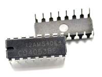
 CD4052资料手册参数详解、引脚配置说明

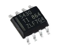
 一文带你了解TPS5430资料手册分析:参数介绍、引脚配置说明
