transmit scheduling upon reception. In addition, a 16-bit
time stamp counter supports real-time applications.
3.13
ANALOG TO DIGITAL CONVERTER
This device contains a 10-channel, multiplexed input, suc-
cessive approximation, 10-bit Analog-to-Digital Converter. It
supports both single-ended and differential modes of oper-
ation.
The CAN modules allow single-cycle byte or word read/
write access. A set of diagnostic features (such as loop-
back, listen only, and error identification) support the devel-
opment with the CAN modules and provide a sophisticated
error management tool.
The integrated 10-bit ADC provides the following features:
10-channel, multiplexed input
5 differential channels
Single-ended and differential external filtering capability
12-bit resolution; 10-bit accuracy
Sign bit
The CAN receivers can trigger a wake-up condition out of
low-power modes through the Multi-Input Wake-Up unit.
3.9
AUDIO/TELEMATICS CODEC
The on-chip codec is designed for voice input and stereo
audio playback. It includes dual mono ADC channels oper-
ating at a sample rate of 8-24 kHz (125× oversampling clock
required). A stereo DAC operates at selected sample rates
from a 125× or 128× oversampling clock, driving two config-
urable, gain-programmable differential line driver outputs.
The DAC features click and pop reduction circuit, zero-
cross detector circuit, tone/compensation filter, sidetone in-
jection from ADC, and internal power management circuit.
The ADCs accept differential or single-ended analog micro-
phone inputs. The DAC employs fully differential signalling
for high PSRR and low crosstalk. DMA transfers are sup-
ported to allow for fast CPU-independent receive and trans-
mit.
10-microsecond conversion time
External start trigger
Programmable start delay after start trigger
Poll or interrupt on conversion completion
The ADC provides several options for the voltage reference
source. The positive reference can be ADVCC (internal),
VREF, ADC0, or ADC1. The negative reference can be AD-
VCC (internal), ADC2, or ADC3.
Two specific analog channel selection modes are support-
ed. These are as follows:
Allow any specific channel to be selected at one time.
The A/D Converter performs the specific conversion re-
quested and stops.
Allow any differential channel pair to be selected at one
time. The A/D Converter performs the specific differential
conversion requested and stops.
3.10
CVSD/PCM CONVERSION MODULES
The two CVSD/PCM modules perform conversion between
CVSD data and PCM data, in which the CVSD encoding is
as defined in the Bluetooth specification and the PCM data
can be 8-bit μ-Law, 8-bit A-Law, or 13-bit to 16-bit Linear.
In both single-ended and differential modes, there is the ca-
pability to connect the analog multiplexer output and A/D
converter input to external pins. This provides the ability to
externally connect a common filter/signal conditioning cir-
cuit for the A/D Converter.
3.11
I2S DIGITAL AUDIO BUS
The Inter-IC Sound (I2S) interface is a synchronous serial
interface intended for the transfer of digital audio data. The
I2S interface can be configured as a master or a slave, and
it supports all three common data formats: I2S-mode, left-
justified, and right-justified. It has programmable word
length from 8 to 32 bits and programmable valid data reso-
lution from 8 to 24 bits.
3.14
QUAD UART
Four UART modules support a wide range of programmable
baud rates and data formats, parity generation, and several
error detection schemes. The baud rate is generated on-
chip, under software control. All UART modules support
DMA and hardware flow control. One module has USART
capability (synchronous mode) at speeds up to 921.6
kbaud. The UARTs offer a wake-up condition from the low-
power modes using the Multi-Input Wake-Up module.
3.12
ADVANCED AUDIO INTERFACE
The Advanced Audio Interface (AAI) provides a serial syn-
chronous, full-duplex interface to codecs and similar serial
devices. Transmit and receive paths operate asynchro-
nously with respect to each other. Each path uses three sig-
nals for communication: shift clock, frame synchronization,
and data.
3.15
MICROWIRE/SPI
The two Microwire/SPI (MWSPI) interface modules support
synchronous serial communications with other devices that
conform to Microwire or Serial Peripheral Interface (SPI)
specifications. It supports 8-bit and 16-bit data transfers.
When the receiver and transmitter use external shift clocks
and frame sync signals, the interface operates in its asyn-
chronous mode. Alternatively, the transmit and receive path
can share the same shift clock and frame sync signals for
synchronous mode operation.
The Microwire interfaces allows several devices to commu-
nicate over a single system consisting of four wires: serial
in, serial out, shift clock, and slave enable. At any given
time, the Microwire interfaces operate as a master or a
slave. The Microwire interfaces supports the full set of slave
select for multi-slave implementation.
In master mode, the shift clock is generated on-chip under
software control. In slave mode, a wake-up out of a low-
power mode may be triggered using the Multi-Input Wake-
Up module.
www.national.com
4


 MAX6675资料手册参数详解、引脚配置说明

 LM258引脚图及功能介绍、主要参数分析

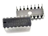
 CD4052资料手册参数详解、引脚配置说明

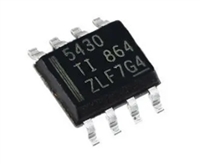
 一文带你了解TPS5430资料手册分析:参数介绍、引脚配置说明
