| 品牌 | Logo | 应用领域 |
| 罗姆 - ROHM | / | |
| 页数 | 文件大小 | 规格书 |
| 39页 | 1653K |  |
| 描述 | ||
| The BD4xxS2-C series are low quiescent regulators featuring 45V absolute maximum voltage, and output voltage accuracy of ±2% (3.3V or 5.0V: Typ), 200mA output current and 40µA (Typ) current consumption. These regulators are therefore ideal for applications requiring a direct connection to the battery and a low current consumption. A logical “HIGH” at the CTL pin enables the device and “LOW” at the CTL pin not enables the device. (Only W: Includes switch) Ceramic capacitors can be used for compensation of the output capacitor phase. Furthermore, these ICs also feature overcurrent protection to protect the device from damage caused by short-circuiting and an integrated thermal shutdown to protect the device from overheating at overload conditions. | ||
| 型号 | 品牌 | 描述 | 获取价格 | 数据表 |
| BD433S2WFP3-C | ROHM | The BD4xxS2-C series are low quiescent regulators featuring 45V absolute maximum voltage, |
获取价格 |

|
| BD433S2WFP3-C (新产品) | ROHM | The BD4xxS2-C series are low quiescent regula |
获取价格 |

|
| BD433S5EFJ-C | ROHM | BD433S5EFJ-C is low quiescent regulators featuring 45V absolute maximum voltage, and outpu |
获取价格 |

|
| BD433S5EFJ-C (新产品) | ROHM | BD433S5EFJ-C is low quiescent regulators feat |
获取价格 |

|
| BD433S5FP2-C | ROHM | BD433S5FP2-C is low quiescent regulators featuring 45V absolute maximum voltage, and outpu |
获取价格 |

|
| BD433S5FP2-C (开发中) | ROHM | BD433S5FP2-C is low quiescent regulators feat |
获取价格 |

|
 MAX6675资料手册参数详解、引脚配置说明

 LM258引脚图及功能介绍、主要参数分析

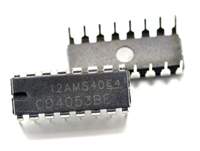
 CD4052资料手册参数详解、引脚配置说明

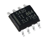
 一文带你了解TPS5430资料手册分析:参数介绍、引脚配置说明
