
| 型号 | 品牌 | 获取价格 | 描述 | 数据表 |
| ADC10D040CIVS | NSC |
获取价格 |
Dual 10-Bit, 40 MSPS, 267 mW A/D Converter |

|
| ADC10D040CIVS/NOPB | TI |
获取价格 |
双通道、10 位、40MSPS 模数转换器 (ADC) | PFB | 48 | -40 |
|
| ADC10D040EVAL | NSC |
获取价格 |
Dual 10-Bit, 40 MSPS, 267 mW A/D Converter |
|
| ADC10D1000 | NSC |
获取价格 |
Low Power, 10-Bit, Dual 1.0/1.5 GSPS or Single 2.0/3.0 GSPS ADC |
|
| ADC10D1000 | TI |
获取价格 |
10 位、双路 1.0GSPS 或单路 2.0GSPS 模数转换器 (ADC) |
|
| ADC10D1000CCMLS | NSC |
获取价格 |
Low Power, 10-Bit, Dual 1.0 GSPS or Single 2.0 GSPS A/DConverter |
|
| ADC10D1000CCMLS | TI |
获取价格 |
耐辐射加固保障 (RHA)、100krad、陶瓷、10 位、双通道 1GSPS 或单通道 |
|
| ADC10D1000CCMPR | NSC |
获取价格 |
Low Power, 10-Bit, Dual 1.0 GSPS or Single 2.0 GSPS A/DConverter |
|
| ADC10D1000CCMPR | TI |
获取价格 |
耐辐射加固保障 (RHA)、100krad、陶瓷、10 位、双通道 1GSPS 或单通道 |
|
| ADC10D1000CCRQV | NSC |
获取价格 |
Low Power, 10-Bit, Dual 1.0 GSPS or Single 2.0 GSPS A/DConverter |
|
 台积电酝酿高端芯片涨价潮!苹果英伟达或面临成本压力

 阿里云紧急辟谣采购寒武纪15万片GPU 国产芯片龙头股价应声大跌
 中国半导体技术全面超越韩国,弯道超车背后的突围密码
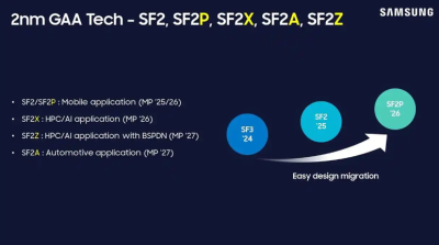 三星第二代2nm工艺SF2P锁定特斯拉AI6 2026年量产存悬念
工作时间:9:00-21:00
CEO邮箱:ceo@jiepei.com
投诉邮箱:tousu@jiepei.com


 浙公网安备 33010502006866号 浙ICP备10014259号-119
营业执照ICP证
浙公网安备 33010502006866号 浙ICP备10014259号-119
营业执照ICP证


