Functional Description
The 74ABT3284 is a bi-directional registered data-path rout-
ing device which can multiplex/de-multiplex four 9-bit ‘‘A-
side’’ data ports (Ports A, B, C, D) onto/from one 9-bit ‘‘X-
side’’ port (Port X). Alternatively, it can be configured for
mux/demux of two 18-bit data paths (Ports A and C, B and
D) onto/from one 18-bit data path (Ports X and Y).
All Data Path Control Inputs and Input/Output Register
Load Enable Inputs are active high and can be asserted
asynchronously or synchronously. When MODE SC is low,
these inputs operate asynchronously. When MODE SC is
Ð
high, the inputs are asserted synchronously on the positive
Ð
edge of the CP IN clock.
Ð
Each of the six 9-bit I/O ports have independent active low
TRI-STATE output enable control logic which can be con-
When operating the Data Path Control and/or the Output
Enable Input groups with MODE SC and/or MODE SO
‘‘hard wired’’ high for synchronous mode, a single pre-clock
É
figured to operate asynchronously or synchronously. With
Ð
Ð
MODE SO low, direct asynchronous output control is pro-
Ð
of CP IN will be required following power-up to insure that
Ð
vided. With MODE SO high, output enable control is as-
Ð
all internal synchronous control registers are in the appropri-
ate known state. if the application requires ‘‘on the fly’’’
changes from asynchronous to synchronous operation,
then the respective control/enable pin data must be pre-
serted synchronously on the positive edge of the CP IN
Ð
clock. All I/O port inputs are continuously active allowing
output state feedback.
clocked via CP IN and held steady prior to and during any
Ð
The four A-side ports (A, B, C, D) contain independently
enabled input and output data registers for storage of data
passing in either direction. The input register (AIR, BIR, CIR,
low to high transition of the MODE SO or MODE SC to
Ð
Ð
properly initiate the sync control registers for synchronous
control mode.
DIR) is loaded/held on the positive edge of CP AX when
Ð
the respective Load Control pin (LDAI, LDBI, LDCI, LDDI) is
asserted high/low. The Input Registers can be loaded with
data from the corresponding A-side port. The output register
(AOR, BOR, COR, DOR) is loaded/held on the positive
Pin Descriptions
Pin Name
Description
Operation
edge of CP XA when the respective Load Control pin
Ð
OEa
Output Enable Inputs
(Active Low)
Sync/Async
(LDAO, LDBO, LDCO, LDDO) is asserted high/low. The
Output Registers can be loaded with data from Port X when
MODE WS is asserted low. When MODE WS is asserted
LDaI
Load Enable Inputs for the
Input Registers
Sync/Async
Sync/Async
Ð
Ð
high, the Output Registers A and C can be loaded with Port
X data and the B and D Output Registers can be loaded with
data from Port Y.
LDaO
Load Enable Inputs for the
Output Registers
When routing data from A-side to X-side, Data Path Control
is provided for the following options via the SA2X inputs;
Transparent mode where Input Register is bypassed but
can simultaneously monitor A-side data; Registered Mode
where X-side receives data from the selected Input Regis-
ters; Readback Mode where X-side receives data from the
selected Output Registers. A-side data from Ports A, B, C,
or D can be selected to Port X via the XSEL data path select
inputs. Ports B or D can be selected to Port Y via the YSEL
data path select input.
ASEL(0,1) A-Side Data Path Select Inputs Sync/Async
SA2X(0,1) X-Side Data Path Select Inputs Sync/Async
XSEL(0,1) X-Port Data Path Select Inputs Sync/Async
YSEL
Y-Port Data Path Select Input
Sync/Async
Sync/Async
MODE
W
Word Mode Select Input for
the X/Y to A-Side Direction
Ð
MODE SO Enable Input for Synchronous
Ð
Output Enable Control
Async
Async
When routing data from X-side to A-side, Data Path Control
is provided for the following options via the ASEL inputs;
Transparent mode where Output Register is bypassed but
can simultaneously monitor X-side data; Registered Mode
where the A-side Port receives data from the corresponding
Output Register; Readback Mode where the A-side Port re-
ceives data from the corresponding Input Registers.
MODE SC Enable Input for Synchronous
Ð
Data Path Control
CP IN
Ð
Clock Input for Synchronous
Control (Positive Edge Trigger)
MODE WS asserted low selects Port X data to be passed
Ð
to Ports A, B, C, and D. With MODE WS asserted high,
Ð
Port X data is passed to Ports A and C with Port Y data
CP AX
Ð
Clock Input for Input Registers
(Positive Edge Trigger)
passed to Ports B and D.
CP XA
Ð
Clock Input for Output Registers
(Positive Edge Trigger)
2


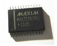
 MAX7219驱动8段数码管详解及数据手册关键信息

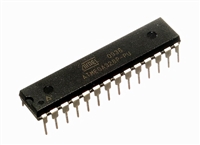
 ATMEGA328P技术资料深入分析

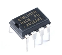
 AT24C02芯片手册管脚信息、参数分析、应用领域详解

 AT24C256芯片手册参数分析、引脚说明、读写程序示例
