ISSP1
High-Speed Interface Family
ISSPSeries
Features (continued)
Description
With multiple high-speed serializer/deserializer (SerDes) transceiver cores built into the
platform, the ISSP1 High-Speed Interface (HSI) family brings fast-throughput capabilities
to NEC Electronics’ Instant Silicon Solutions Platform™ (ISSP™). Like all ISSP1 products,
the ISSP1-HSI devices take advantage of NEC Electronics’ 150 nm (UX4) CMOS process
for implementing complex ASIC designs with global clock frequencies as high as 250
MHz and much higher rates for SerDes operation. ISSP delivers close to cell-based ASIC
performance levels with a complex multi-gate (CMG) based logic fabric that delivers high
performance and low power. The ISSP prefabricated architecture incorporates clock
domains, design-for-test circuitry, global routes, and other resources into the fabric of the
chip. This architecture simplies the design flow and enables exceptionally fast manufac-
turing turnaround.
Design Performance,
Turnaround Time
Advantage
The SerDes cores in ISSP1-HSI devices support data rates ranging from 622 Mbps to
3.125 Gbps and comply with physical-layer standards for PCI Express™, XAUI, Gigabit
Ethernet and Fibre Channel. Since the SerDes cores are incorporated in the ISSP1-HSI
architecture, signal integrity is assured.
Other IP in the platform's prefabricated structure includes multiple SRAM blocks and
high-speed analog phase-locked loops (APLLs) with phase-shift capability for versatile
clock generation. An embedded clock structure enables design with predictable and
minimized clock skew. Since several types of design-for-test (DFT) circuits are embed-
ded in every ISSP1-HSI master, there is no danger of functional or timing resimulations
after test insertion. An embedded power mesh means fewer power integrity issues.
Additionally, the architecture provides a large array of complex multi-gates for implement-
ing custom logic. The use of complex logic elements makes it possible to optimize
transistor sizes for different functions, thus improving custom logic performance.
Block Diagram
With many elements traditionally executed in the ASIC design flow embedded into its
architecture, ISSP has a greatly simplifed design flow that minimizes design iterations.
The entire base master architecture has been preverified to eliminate signal integrity
issues that can result in development delays. As a result, ISSP1-HSI devices enable a
much shorter design cycle than cell-based ASICs. Manufacturing time is extremely short
because only two metal layers must be added to customize an ISSP1-HSI master with a
custom logic design.
Low-Risk Advantage
Advantages
By providing a fast-turn solution with low NRE costs, ISSP1-HSI makes it practical to
develop high-performance ASICs for modest production volumes. If volumes need to
increase, the design can migrate easily to an NEC Electronics cell-based ASIC product
using the same process technology and based on the same IP and design flow.
• Embedded SerDes cores for easy implementation of high-speed data interfaces
• Low overall development costs, engineering resources and mask NRE expenses for
quick ROI
• Built-in DFT circuits, clocks, SRAM, signal integrity assurance and other features that
simplify the design process and boost performance
• Logic structure with optimized transistor sizes to improve design performance
• Mid-volume production capabilities with extremely fast turnaround times
• Predictable flow for layout and turnaround times
• Ability to leverage cell-based IP for easy migration to cell-based ASICs


 纳微科技震撼发布GaNSlim革新氮化镓功率芯片

 意法半导体发布第四代SiC技术,助力电动汽车电驱

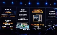
 联发科推出全球首款3纳米汽车芯片CT-X1,挑战高通SA8295

 国家大基金减持三家半导体企业,市场反应各异
