
 5秒后页面跳转

| 是否Rohs认证: | 符合 | 生命周期: | Active |
| 零件包装代码: | LGA | 包装说明: | LGA-32 |
| 针数: | 32 | Reach Compliance Code: | compliant |
| HTS代码: | 8542.39.00.01 | 风险等级: | 1.48 |
| 应用程序: | SONET;SDH | 长度: | 5 mm |
| 湿度敏感等级: | 3 | 功能数量: | 1 |
| 端子数量: | 32 | 最高工作温度: | 95 °C |
| 最低工作温度: | -40 °C | 封装主体材料: | UNSPECIFIED |
| 封装代码: | VBCC | 封装形式: | CHIP CARRIER |
| 认证状态: | Not Qualified | 座面最大高度: | 0.95 mm |
| 标称供电电压: | 1.8 V | 表面贴装: | YES |
| 电信集成电路类型: | ATM/SONET/SDH TRANSCEIVER | 温度等级: | INDUSTRIAL |
| 端子形式: | BUTT | 端子节距: | 0.5 mm |
| 端子位置: | BOTTOM | 宽度: | 5 mm |
| Base Number Matches: | 1 |
| 型号 | 品牌 | 获取价格 | 描述 | 数据表 |
| SI504-EVB | SILICON |
获取价格 |
USB plug-in board that allows for evaluation of the Si50x family of CMEMS oscillators. |

|
| SI510 | SILICON |
获取价格 |
CRYSTAL OSCILLATOR 100 kHZ TO 250 MHZ |
|
| SI5100 | SILICON |
获取价格 |
SiPHY⑩ OC-48/STM-16 SONET/SDH TRANSCEIVER |
|
| SI-51002 | BEL |
获取价格 |
SI-51002 |
|
| SI-51002-F | BEL |
获取价格 |
SI-51002-F |
|
| SI-51002-G | BEL |
获取价格 |
Telecom and Datacom Connector |
|
| SI-51003 | BEL |
获取价格 |
SI-51003 |
|
| SI-51003-F | BEL |
获取价格 |
SI-51003-F |
|
| SI-51004 | BEL |
获取价格 |
SI-51004 |
|
| SI-51005-CB | BEL |
获取价格 |
Telecom and Datacom Connector, ROHS COMPLIANT |
|
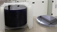 晶圆厂易主:Coherent公司2000万英镑出售苹果供应链关键资产

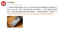 Galaxy S25系列或全系搭载骁龙8 Elite
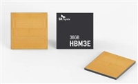 三大厂商12层HBM3E进展迅速
 塔塔电子与力积电达成技术转让协议,携手建设印度首座晶圆厂
工作时间:9:00-21:00
CEO邮箱:ceo@jiepei.com
投诉邮箱:tousu@jiepei.com


 浙公网安备 33010502006866号 浙ICP备10014259号-119
营业执照ICP证
浙公网安备 33010502006866号 浙ICP备10014259号-119
营业执照ICP证


