Features
•
Multiple-mapping support and mapping-based block access timing (0–31 additional cycles)
allowing use for emulation of other memory types
•
•
•
Software programmable block program/erase restriction control
ECC with single-bit correction, double-bit detection
Minimum program size is two consecutive 32-bit words, aligned on a 0-modulo-8 byte address
(due to ECC)
•
•
•
•
Embedded hardware program and erase algorithm
Erase suspend, program suspend and erase-suspended program
Shadow information stored in non-volatile shadow block
Independent program/erase of the shadow block
2.5.3
General-purpose static RAM (SRAM)
The PXR40 SRAM module provides an internal general-purpose 256 KB memory block. The SRAM
controller includes these features:
•
•
•
•
•
Supports read/write accesses mapped to the SRAM memory from any master
32 KB block powered by separate supply for standby operation (contents retained)
Byte, halfword, word, and doubleword addressable
ECC performs single-bit correction, double-bit detection on 64-bit data elements
ECC single-bit error corrections are optionally visible to software
2.5.4
Error correction status module (ECSM)
The error correction status module (ECSM) provides the following:
•
Status information regarding platform memory errors reported by error detection code (EDC) and
error correcting code (ECC) hardware
— Single-bit correction reporting for SRAM and flash memory
— Multi-bit error reporting
•
Includes facilities to allow CPU software to test the error ECC and EDC operation for on-chip
memories by supporting injection of arbitrary error patterns
2.5.5
Enhanced modular input output system (Timer—eMIOS)
The eMIOS module provides the functionality to generate or measure time events. A unified channel (UC)
module is employed that provides a superset of the functionality of all of the MIOS channels used on
MPC5500 family devices, while providing a consistent user interface. This allows more flexibility as each
unified channel can be programmed for different functions in different applications. To identify as many
as two timed events, each UC contains two comparators, a time base selector and registers. This structure
is able to produce match-events, which can be configured to measure or generate a waveform.
PXR40 Product Brief, Rev. 1
Freescale Semiconductor
Preliminary—Subject to Change Without Notice
7


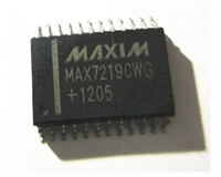
 MAX7219驱动8段数码管详解及数据手册关键信息

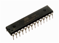
 ATMEGA328P技术资料深入分析

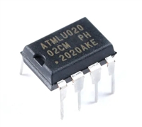
 AT24C02芯片手册管脚信息、参数分析、应用领域详解

 AT24C256芯片手册参数分析、引脚说明、读写程序示例
