
 5秒后页面跳转

| 是否无铅: | 不含铅 | 生命周期: | Active |
| 包装说明: | , | Reach Compliance Code: | not_compliant |
| Factory Lead Time: | 4 weeks | 风险等级: | 5.66 |
| JESD-609代码: | e3 | 湿度敏感等级: | 1 |
| 峰值回流温度(摄氏度): | 260 | 端子面层: | Tin (Sn) |
| 处于峰值回流温度下的最长时间: | 30 | Base Number Matches: | 1 |
| 型号 | 品牌 | 获取价格 | 描述 | 数据表 |
| NVMFS5C645NL | ONSEMI |
获取价格 |
Power MOSFET 2 Amps, 12 Volts |

|
| NVMFS5C645NL_17 | ONSEMI |
获取价格 |
Power MOSFET |
|
| NVMFS5C645NLAFT1G | ONSEMI |
获取价格 |
Power MOSFET |
|
| NVMFS5C645NLT1G | ONSEMI |
获取价格 |
Power MOSFET |
|
| NVMFS5C645NLT3G | ONSEMI |
获取价格 |
Power MOSFET |
|
| NVMFS5C645NLWFAFT1G | ONSEMI |
获取价格 |
Power MOSFET |
|
| NVMFS5C645NLWFT1G | ONSEMI |
获取价格 |
Power MOSFET |
|
| NVMFS5C645NLWFT3G | ONSEMI |
获取价格 |
Power MOSFET |
|
| NVMFS5C645NT1G | ONSEMI |
获取价格 |
单 N 沟道,功率 MOSFET,60V,92A,4.6mΩ |
|
| NVMFS5C645NWFT1G | ONSEMI |
获取价格 |
单 N 沟道,功率 MOSFET,60V,92A,4.6mΩ |
|
 DS1135-8资料手册解读:深入探索高速硅定时电路的特性与应用

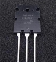 GT60N321资料手册解读:深入了解东芝第四代绝缘栅双极晶体管
 STS5DNE30L资料手册解读:参数分析、特性与应用
 MDU1511资料手册解读:探索这款MOSFET的全面特性
工作时间:9:00-21:00
CEO邮箱:ceo@jiepei.com
投诉邮箱:tousu@jiepei.com


 浙公网安备 33010502006866号 浙ICP备10014259号-119
营业执照ICP证
浙公网安备 33010502006866号 浙ICP备10014259号-119
营业执照ICP证


