MC9S08DZ60 Series Features
8-Bit HCS08 Central Processor Unit (CPU)
Peripherals
• 40-MHz HCS08 CPU (20-MHz bus)
• ADC — 24-channel, 12-bit resolution, 2.5 μs
conversion time, automatic compare function,
temperature sensor, internal bandgap reference channel
• HC08 instruction set with added BGND instruction
• Support for up to 32 interrupt/reset sources
• ACMPx — Two analog comparators with selectable
interrupt on rising, falling, or either edge of comparator
output; compare option to fixed internal bandgap
reference voltage
On-Chip Memory
• Flash read/program/erase over full operating voltage and
temperature
• MSCAN — CAN protocol - Version 2.0 A, B; standard
and extended data frames; Support for remote frames;
Five receive buffers with FIFO storage scheme; Flexible
identifier acceptance filters programmable as: 2 x 32-bit,
4 x 16-bit, or 8 x 8-bit
— MC9S08DZ60 = 60K
— MC9S08DZ48 = 48K
— MC9S08DZ32 = 32K
— MC9S08DZ16 = 16K
• Up to 2K EEPROM in-circuit programmable memory;
8-byte single-page or 4-byte dual-page erase sector;
Program and Erase while executing Flash; Erase abort
• SCIx — Two SCIs supporting LIN 2.0 Protocol and
SAE J2602 protocols; Full duplex non-return to zero
(NRZ); Master extended break generation; Slave
extended break detection; Wakeup on active edge
• Up to 4K random-access memory (RAM)
• SPI — Full-duplex or single-wire bidirectional;
Double-buffered transmit and receive; Master or Slave
mode; MSB-first or LSB-first shifting
Power-Saving Modes
• Two very low power stop modes
• Reduced power wait mode
• IIC — Up to 100 kbps with maximum bus loading;
Multi-master operation; Programmable slave address;
General Call Address; Interrupt driven byte-by-byte data
transfer
• Very low power real time interrupt for use in run, wait,
and stop
Clock Source Options
• TPMx — One 6-channel (TPM1) and one 2-channel
(TPM2); Selectable input capture, output compare, or
buffered edge-aligned PWM on each channel
• Oscillator (XOSC) — Loop-control Pierce oscillator;
Crystal or ceramic resonator range of 31.25 kHz to
38.4 kHz or 1 MHz to 16 MHz
• RTC — (Real-time counter) 8-bit modulus counter with
binary or decimal based prescaler; Real-time clock
capabilities using external crystal and RTC for precise
time base, time-of-day, calendar or task scheduling
functions; Free running on-chip low power oscillator
(1 kHz) for cyclic wake-up without external components
• Multi-purpose Clock Generator (MCG) — PLL and
FLL modes (FLL capable of 1.5% deviation using
internal temperature compensation); Internal reference
clock with trim adjustment (trimmed at factory, with
trim value stored in flash); External reference with
oscillator/resonator options
Input/Output
System Protection
• 53 general-purpose input/output (I/O) pins and 1
input-only pin
• Watchdog computer operating properly (COP) reset
with option to run from backup dedicated 1-kHz internal
clock source or bus clock
• 24 interrupt pins with selectable polarity on each pin
• Hysteresis and configurable pull device on all input pins.
• Configurable slew rate and drive strength on all output
pins.
• Low-voltage detection with reset or interrupt; selectable
trip points
• Illegal opcode detection with reset
• Illegal address detection with reset
• Flash block protect
Package Options
• 64-pin low-profile quad flat-pack (LQFP) — 10x10 mm
• 48-pin low-profile quad flat-pack (LQFP) — 7x7 mm
• 32-pin low-profile quad flat-pack (LQFP) — 7x7 mm
• Loss-of-lock protection
Development Support
• Single-wire background debug interface
• On-chip, in-circuit emulation (ICE) with real-time bus capture


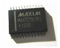
 MAX7219驱动8段数码管详解及数据手册关键信息

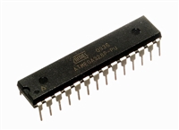
 ATMEGA328P技术资料深入分析

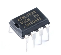
 AT24C02芯片手册管脚信息、参数分析、应用领域详解

 AT24C256芯片手册参数分析、引脚说明、读写程序示例
