LNK403-409/413-419
start-up C4 is charged to ~6 V from an internal high-voltage
current source tied to the device DRAIN pin. Once the bias
voltage has risen into regulation the operating supply current is
provided via R10. Diode D4 prevents U1 from charging C6
during start-up which would increase the start-up delay time.
100 mF BYPASS pin capacitor for all but the LNK4x3 which has
only one power setting. In all cases in order to obtain the best
output current tolerance maintain the device temperature below
100 °C
Maximum Input Capacitance
Feedback
To achieve high power factor, the capacitance used in both the
EMI filter and for decoupling the rectified AC (bulk capacitor)
must be limited in value. The maximum value is a function of
the output power of the design and reduces as the output
power reduces. For the majority of designs limit the total
capacitance to less than 200 nF with a bulk capacitor value of
100 nF. Film capacitors are recommended compared to
ceramic types as they minimize audible noise with operating
with leading edge phase dimmers. Start with a value of 10 nF
for the capacitance in the EMI filter and increase in value until
there is sufficient EMI margin.
The bias winding voltage is proportional to the output voltage
(set by the turns ratio between the bias and secondary
windings). This allows the output voltage to be monitored
without secondary side feedback components. Resistor R15
converts the bias voltage into a current which is fed into the
FEEDBACK pin of U1. The internal engine within U1 combines
the FEEDBACK pin current, VOLTAGE MONITOR pin current
and drain current information to provide a constant output
current over a 2:1 output voltage range.
Output Rectification
The transformer secondary winding is rectified by D2 and
filtered by C4 and C5. A Schottky barrier diode was selected
for efficiency and the combined value of C4 and C5 were
selected to give an acceptable LED ripple current. For designs
where lower ripple is desirable the output capacitance value
can be increased. A small pre-load is provided by R6 which
limits the output voltage under no-load conditions.
REFERENCE Pin Resistance Value Selection
The LinkSwitch-PH family contains phase dimming devices,
LNK403-409, and non-dimming devices, LNK413-419. The
non-dimmable devices use a 24.9 kW 1% REFERENCE pin
resistor in high-line and universal input voltage designs and
49.9 kW 1% in low-line input voltage designs, for best output
current tolerance (over AC input voltage changes). The dimmable
devices use 49.9 kW 1% to achieve the widest dimming range.
Key Application Considerations
VOLTAGE MONITOR Pin Resistance Network Selection
For widest AC phase angle dimming range with LNK403-409,
use a 4 MW resistor connected to the line voltage peak detector
circuit. Make sure that the resistor’s voltage rating is sufficient
for the peak line voltage. If necessary use multiple series
connected resistors.
Power Table
The data sheet power table (Table 1) represents the minimum
and maximum practical continuous output power based on the
following conditions:
1. Efficiency of 80%
2. Device local ambient of 70 °C
3. Sufficient heat sinking to keep the device temperature
below 100 °C
For best line regulation, use a series combination of resistors
that equals 3.909 MW connected to the line voltage peak
detector. In addition, connect a 1 MW in series with a 402 kW
resistor (1.402 MW total) from the VOLTAGE MONITOR pin to
SOURCE pin. Use 1% tolerance resistors for good accuracy.
Line regulation can be further improved by using the PIXls
spreadsheet’s fine tuning section. See the LinkSwitch-PH
Application Note for more information.
4. For minimum output power column
•ꢀ Reflected output voltage (VOR) of 120 V
•ꢀ FEEDBACK pin current of 135 mA
•ꢀ BYPASS pin capacitor value of 10 mF
5. For maximum output power column
•ꢀ Reflected output voltage (VOR) of 65 V
•ꢀ FEEDBACK pin current of 165 mA
•ꢀ BYPASS pin capacitor value of 100 mF
(LNK4x3EG = 10 mF)
Primary Clamp and Output Reflected Voltage VOR
A primary clamp is necessary to limit the peak drain to source
voltage. A Zener clamp requires the fewest components and
board space and gives the highest efficiency. RCD clamps are
also acceptable however the peak drain voltage should be
carefully verified during start-up and output short-circuit as the
clamping voltage varies with significantly with the peak drain
current.
Note that input line voltages above 85 VAC do not change the
power delivery capability of LinkSwitch-PH devices.
Device Selection
Select the device size by comparing the required output power
to the values in Table 1. For thermally challenging designs, e.g.
incandescent lamp replacement, where either the ambient
temperature local to the LinkSwitch-PH device is high and/or
there is minimal space for heat sinking use the minimum output
power column. This is selected by using a 10 mF BYPASS pin
capacitor and results in a lower device current limit and
therefore lower conduction losses. For open frame design or
designs where space is available for heat sinking then refer to
the maximum output power column. This is selected by using a
For the highest efficiency, the clamping voltage should be
selected to be at least 1.5 times the output reflected voltage,
VOR, as this keeps the leakage spike conduction time short.
When using a Zener clamp in a universal input or high-line only
application, a VOR of less than 135 V is recommended to allow
for the absolute tolerances and temperature variations of the
Zener. This will ensure efficient operation of the clamp circuit
and will also keep the maximum drain voltage below the rated
breakdown voltage of the FET. An RCD (or RCDZ) clamp
8
Rev. D 08/11
www.powerint.com


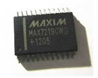
 MAX7219驱动8段数码管详解及数据手册关键信息

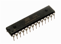
 ATMEGA328P技术资料深入分析

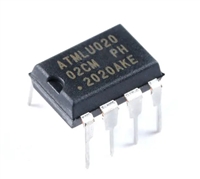
 AT24C02芯片手册管脚信息、参数分析、应用领域详解

 AT24C256芯片手册参数分析、引脚说明、读写程序示例
