
 5秒后页面跳转

| 型号 | 品牌 | 获取价格 | 描述 | 数据表 |
| DS90UR124IVS | NSC |
获取价格 |
5-43 MHz DC-Balanced 24-Bit LVDS Serializer and Deserializer |

|
| DS90UR124IVS/NOPB | TI |
获取价格 |
5MHz 至 43MHz 直流平衡 24 位 FPD-Link II 解串器 | PAG |
|
| DS90UR124IVSX | NSC |
获取价格 |
5-43 MHz DC-Balanced 24-Bit LVDS Serializer and Deserializer |
|
| DS90UR124IVSX/NOPB | NSC |
获取价格 |
IC LINE TRANSCEIVER, QFP64, 10 X 10 MM, 1 MM HEIGHT, 0.50 PITCH, ROHS COMPLIANT, TQFP-64, |
|
| DS90UR124IVSX/NOPB | TI |
获取价格 |
5MHz 至 43MHz 直流平衡 24 位 FPD-Link II 解串器 | PAG |
|
| DS90UR124Q | NSC |
获取价格 |
5-43 MHz DC-Balanced 24-Bit FPD-Link II Serializer and Deserializer Chipset |
|
| DS90UR124-Q1 | TI |
获取价格 |
5MHz 至 43MHz 直流平衡 24 位 FPD-Link II 解串器 - 汽车级 |
|
| DS90UR124QVS | NSC |
获取价格 |
5-43 MHz DC-Balanced 24-Bit FPD-Link II Serializer and Deserializer Chipset |
|
| DS90UR124QVS/NOPB | TI |
获取价格 |
5MHz 至 43MHz 直流平衡 24 位 FPD-Link II 解串器 - 汽车级 |
|
| DS90UR124QVSX | NSC |
获取价格 |
5-43 MHz DC-Balanced 24-Bit FPD-Link II Serializer and Deserializer Chipset |
|
 解析BAV99LT1G手册:参数分析、替换型号推荐

 解读BSS138PW数据手册:产品特性、电气参数及替换型号推荐
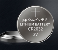 CR2032资料手册解读:参数分析、替换型号推荐
 CDSOT23-SM712参数分析、替代型号推荐
工作时间:9:00-21:00
CEO邮箱:ceo@jiepei.com
投诉邮箱:tousu@jiepei.com


 浙公网安备 33010502006866号 浙ICP备10014259号-119
营业执照ICP证
浙公网安备 33010502006866号 浙ICP备10014259号-119
营业执照ICP证


