ADS131E08S
ZHCSEJ3B –JUNE 2015–REVISED APRIL 2020
www.ti.com.cn
Pin Functions (continued)
PIN
TYPE
DESCRIPTION
NAME
START
NO.
38
18
17
28
30
55
26
25
24
Digital input
Analog input/output
Analog input/output
Analog output
Analog output
Analog output
Analog output
Analog input
Start conversion
TESTN(1)
TESTP(1)
VCAP1
VCAP2
VCAP3
VCAP4
VREFN
VREFP
Test signal, negative pin; connect to DGND with a 10-kΩ resistor if unused
Test signal, positive pin; connect to DGND with a 10-kΩ resistor if unused
Analog bypass capacitor; connect a 470-pF capacitor to AVSS
Analog bypass capacitor; connect a 270-nF capacitor to AVSS
Analog bypass capacitor; connect a 270-nF capacitor to AVSS
Analog bypass capacitor; connect a 270-nF capacitor to AVSS
Negative reference voltage; connect to AVSS
Analog output
Positive reference voltage output; connect a 330-nF capacitor to VREFN
7 Specifications
7.1 Absolute Maximum Ratings
over operating ambient temperature range (unless otherwise noted)(1)
MIN
–0.3
MAX
5.5
UNIT
V
AVDD to AVSS
DVDD to DGND
–0.3
3.9
V
AVSS to DGND
–3
0.2
V
Analog input voltage
AVSS – 0.3
DGND – 0.3
DGND – 0.3
–10
AVDD + 0.3
DVDD + 0.3
DVDD + 0.3
10
V
Digital input voltage
V
Digital output voltage
V
Continuous input current to any pin except supply pins(2)
Junction temperature, TJ
Storage temperature, Tstg
mA
°C
°C
–40
150
–60
150
(1) Stresses beyond those listed under Absolute Maximum Ratings may cause permanent damage to the device. These are stress ratings
only, which do not imply functional operation of the device at these or any other conditions beyond those indicated under Recommended
Operating Conditions. Exposure to absolute-maximum-rated conditions for extended periods may affect device reliability.
(2) Input pins are diode-clamped to the power-supply rails. Input signals that can swing beyond the supply rails must be current limited to 10
mA or less.
7.2 ESD Ratings
VALUE
UNIT
Human-body model (HBM), per ANSI/ESDA/JEDEC JS-001(1)
±2000
V(ESD)
Electrostatic discharge
V
Charged-device model (CDM), per JEDEC specification JESD22-C101 or
ANSI/ESDA/JEDEC JS-002(2)
±500
(1) JEDEC document JEP155 states that 500 V HBM allows safe manufacturing with a standard ESD control process.
(2) JEDEC document JEP157 states that 250 V CDM allows safe manufacturing with a standard ESD control process.
6
Copyright © 2015–2020, Texas Instruments Incorporated


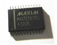
 MAX7219驱动8段数码管详解及数据手册关键信息

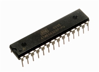
 ATMEGA328P技术资料深入分析

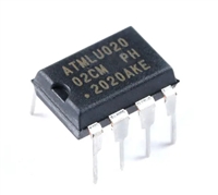
 AT24C02芯片手册管脚信息、参数分析、应用领域详解

 AT24C256芯片手册参数分析、引脚说明、读写程序示例
