ADS131B24-Q1
www.ti.com.cn
UNIT
ZHCSN80 – JULY 2023
7.4 Thermal Information
TQFP (PHP)
48 PINS
23.7
THERMAL METRIC(1)
RθJA
Junction-to-ambient thermal resistance
Junction-to-case (top) thermal resistance
°C/W
°C/W
°C/W
°C/W
°C/W
°C/W
RθJC(top)
RθJB
15.3
Junction-to-board thermal resistance
7.8
ΨJT
Junction-to-top characterization parameter
Junction-to-board characterization parameter
Junction-to-case (bottom) thermal resistance
0.2
ΨJB
7.7
RθJC(bot)
1.3
(1) For more information about traditional and new thermal metrics, see the Semiconductor and IC Package Thermal Metrics application
report.
7.5 Electrical Characteristics
minimum and maximum specifications apply from TA = –40°C to +105°C; typical specifications are at TA = 25°C; all
specifications are at APWR = 5 V, DPWR = 5 V, IOVDD = 3.3 V, external clock, fCLK = 8.192 MHz, global-chop mode
disabled, ADC1y data rate = 1 kSPS (unless otherwise noted)
PARAMETER
CURRENT MEASUREMENT ADCS (ADC1A, ADC1B)
Resolution
TEST CONDITIONS
MIN
TYP
MAX
UNIT
24
Bits
V/V
Gain settings
4, 8, 16, 32
fDATA
Output data rate
fCLK = 8.192 MHz
500
64k
5
SPS
All data rates, all gains, global-chop enabled or
disabled, VCPy = VCNy = 0 V
Absolute input current
±0.5
±1
nA
nA
All data rates, all gains, global-chop enabled or
disabled, VCPy = VCNy = 0 V
Differential input current
–5
All data rates, all gains, global-chop enabled or
disabled
Differential input impedance
1.8
MΩ
Gain = 4, global-chop disabled
Gain = 8 to 32, global-chop disabled
All gains, global-chop enabled
All gains, global-chop disabled
All gains, global-chop enabled
±1
±15
±0.5
20
Offset error (input referred)
µV
–1.5
1.5
100
7
Offset drift
Gain error
nV/°C
1
TA = 25°C, all gains, single-ended operation with
CNy held at AGNDy, including initial accuracy of
REFy
–0.15%
±0.05%
0.15%
All gains, single-ended operation with CNy held
at AGNDy, including drift of REFy
Gain drift
5
20 ppm/°C
ppm
1000 hours at 85°C,
all gains, including long-term drift of REFy
Gain long-term drift
±100
Gain match
Between gain settings
–0.12%
±0.03%
0.65
110
0.12%
Noise (input referred)
Gain = 8, fDATA = 1 kSPS
µVRMS
dB
At DC, global-chop disabled
CMRR
PSRR
Common-mode rejection ratio
Power-supply rejection ratio
At DC, global-chop enabled
113
APWR at DC, global-chop enabled or disabled
DPWR at DC, global-chop enabled or disabled
AVDD at DC, global-chop enabled or disabled
IOVDD at DC, global-chop enabled or disabled
133
133
dB
115
131
Copyright © 2023 Texas Instruments Incorporated
English Data Sheet: SBASAA4
8
Submit Document Feedback
Product Folder Links: ADS131B24-Q1


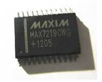
 MAX7219驱动8段数码管详解及数据手册关键信息

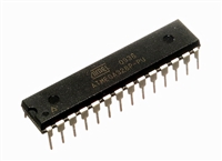
 ATMEGA328P技术资料深入分析

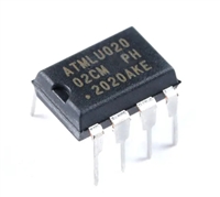
 AT24C02芯片手册管脚信息、参数分析、应用领域详解

 AT24C256芯片手册参数分析、引脚说明、读写程序示例
