B
u
r
r
Ć
B
r
o
w
n
P
r
o
d
u
c
t
s
ADS1282
f
r
o
m
T
e
x
a
s
I
n
s
t
r
u
m
e
n
t
s
SBAS418A–SEPTEMBER 2007–REVISED DECEMBER 2007
High-Resolution Analog-to-Digital Converter
1
FEATURES
DESCRIPTION
2
•
High Resolution:
The ADS1282 is an extremely high-performance,
single-chip analog-to-digital converter (ADC) with an
integrated, low-noise programmable gain amplifier
(PGA) and two-channel input MUX. The ADS1282 is
suitable for the demanding needs of energy
exploration and seismic monitoring environments.
–130dB SNR (250SPS, High-Resolution Mode)
–127dB SNR (250SPS, Low-Power Mode)
•
High Accuracy:
THD: –120dB
INL: 0.8ppm
The converter uses a fourth-order, inherently stable,
delta-sigma (ΔΣ) modulator that provides outstanding
noise and linearity performance. The modulator is
used either in conjunction with the on-chip digital
filter, or can be bypassed for use with post
processing filters.
•
•
•
Low-Noise PGA
Two-Channel Input MUX
Inherently-Stable Modulator with Fast
Responding Over-Range Detection
•
Flexible Digital Filter:
Sinc + FIR + IIR (Selectable)
The flexible input MUX provides an additional
external input for measurement, as well as internal
self-test connections. The PGA features very low
noise (4nV/√Hz) and high input impedance, allowing
easy interfacing to geophones and hydrophones.
Linear or Minimum Phase Response
Programmable High-Pass Filter
Selectable FIR Data Rates: 250SPS to 4kSPS
•
•
Filter Bypass Option
The digital filter provides selectable data rates from
250 to 4000 samples per second (SPS). The
high-pass filter (HPF) features an adjustable corner
frequency. On-chip gain and offset scaling registers
supports system calibration.
Low Power Consumption:
High-Resolution Mode: 27mW
Low-Power Mode: 16mW
Shutdown: 10µW
•
•
•
Offset and Gain Calibration Engine
Synchronization Input
The synchronization input (SYNC) can be used to
synchronize the conversions of multiple ADS1282s.
The SYNC input also accepts a clock input for
continuous alignment of conversions from an external
source.
Analog Supply:
Unipolar (+5V) or Bipolar (±2.5V)
•
Digital Supply: 1.8V to 3.3V
Two operating modes allow optimization of noise and
power. Together, the amplifier, modulator, and filter
dissipate 27mW and only 16mW in low-power mode.
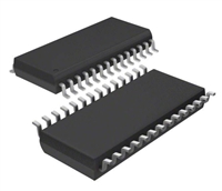
The ADS1282 is available in a compact TSSOP-28
package and is fully specified from –40°C to +85°C,
with a maximum operating range to +125°C.
APPLICATIONS
•
•
•
Energy Exploration
Seismic Monitoring
High-Accuracy Instrumentation
AVDD
PGA
VREFN VREFP
DVDD
CLK
ADS1282
SCLK
DOUT
DIN
Input 1
4th-Order
DS
Programmable
Digital Filter
SPI
Calibration
Interface
Input 2
Modulator
DRDY
VCOM
Over-Range
SYNC
RESET
PWDN
Control
Modulator Output
3
AVSS
DGND
1
Please be aware that an important notice concerning availability, standard warranty, and use in critical applications of
Texas Instruments semiconductor products and disclaimers thereto appears at the end of this data sheet.
2
All trademarks are the property of their respective owners.
PRODUCT PREVIEW information concerns products in the
formative or design phase of development. Characteristic data and
other specifications are design goals. Texas Instruments reserves
the right to change or discontinue these products without notice.
Copyright © 2007, Texas Instruments Incorporated


 ADS1282资料手册解读:主要特征、引脚信息、电气参数

 三星深化印度制造布局,供应链本地化进程加速

 芯擎科技“星辰一号”自动驾驶芯片点亮成功,2025年量产在即

 纳微科技震撼发布GaNSlim革新氮化镓功率芯片
