ADMCF341
PIN FUNCTION DESCRIPTION
Table II. Program Memory Map
The ADMCF341 is available in a 28-lead SOIC package.
Table I describes the pins.
Memory
Type
Address Range
Function
Table I. Pin List
0x0000–0x002F
0x0030–0x01FF
0x0200–0x07FF
0x0800–0x17FF
0x1800–0x1FFF
0x2000–0x20FF
RAM
RAM
Internal Vector Table
User Program Memory
Reserved
Reserved Program Memory
Reserved
User Program Memory
Sector 0
User Program Memory
Sector 1
User Program Memory
Sector 2
Pin Group
Name
No. of Input/
Pins
Output Function
ROM
RESET
1
2
I
Processor Reset Input
SPORT11
I/O
Serial Port 1 Pins (DT1/FL1,
DR1, SCLK1/SCLK02)
Serial Port 0 Pins (DT0, DR0
TFSO, SCLK1/SCLK02)
Processor Clock Output
External Clock or Quartz
Crystal Connection Point
Digital I/O Port Pins
FLASH
FLASH
FLASH
SPORT01
5
I/O
0x2100–0x21FF
0x2200–0x2FFF
0x3000–0x3FFF
CLKOUT
CLKIN, XTAL
11
2
I/O
I, O
Reserved
PORTA0–
PORTA81
AUX0–AUX11
AH–CL
PWMTRIP
ISENSE1–
9
I/O
Table III. Data Memory Map
Memory
2
6
1
3
O
O
I
Auxiliary PWM Outputs
PWM Outputs
PWM Trip Signal
ISENSE Inputs
Address Range
Type
Function
I
0x0000–0x1FFF
0x2000–0x20FF
0x2100–0x37FF
0x3800–0x39FF
0x3A00–0x3BFF
0x3C00–0x3FFF
Reserved
Memory Mapped Registers
Reserved
User Data Memory
Reserved
Memory Mapped Registers
ISENSE
3
VAUX0–VAUX2
ICONST
3
1
I
O
Auxiliary Analog Inputs
ADC Constant Current
Source
Power Supply
Ground
RAM
RAM
VDD
GND
1
1
I
I
NOTES
1Multiplexed pins, individually selectable through PORTA_SELECT
and PORTA_DATA registers.
FLASH MEMORY SUBSYSTEM
The ADMCF341 has 4K ϫ 24-bits of user-programmable,
nonvolatile flash memory. A flash programming utility is pro-
vided with the development tools, which perform the basic
device programming operations: erase, program, and verify.
2SCLK1/SCLK0 multiplexed signals. Selectable through MODECTRL
Register Bit 4.
INTERRUPT OVERVIEW
The flash memory array is portioned into three asymmetrically
sized sectors of 256 words, 256 words, and 3584 words, labeled
sector 0, sector 1, and sector 2, respectively. These sectors are
mapped into external program memory address space.
The ADMCF341 can respond to 18 different interrupt sources
with minimal overhead, seven of which are internal DSP core
interrupts and 11 from the motor control peripherals. The
seven DSP core interrupts are SPORT1 receive (or IRQ0) and
transmit (or IRQ1), SPORT0 receive and transmit, the internal
timer, and two software interrupts. The motor control periph-
eral interrupts are the nine programmable I/Os and two from
the PWM (PWMSYNC pulse and PWMTRIP). All motor
control interrupts are multiplexed into the DSP core through
the peripheral IRQ2 interrupt. The interrupts are internally
prioritized and individually maskable. A detailed description of the
entire interrupt system of the ADMCF341 is presented later,
following a more detailed description of each peripheral block.
Four flash memory interface registers are connected to the DSP.
These 16-bit registers are mapped into the register area of data
memory space. They are named flash memory control register
(FMCR), flash memory address register (FMAR), flash memory
data register low (FMDRL), and flash memory data register
high (FMDRH). These registers are diagrammed later in this
data sheet. They are used by the flash memory programming
utility. The user program may read these registers, but should
not modify them directly. The flash programming utility pro-
vides a complete interface to the flash memory.
MEMORY MAP
It should be noted that the core accesses flash memory through
an external memory interface that multiplexes the program
memory and data memory buses into a single external bus.
Therefore, if more than one external transfer must be made in
the same instruction, there will be at least an overhead cycle
required.
The ADMCF341 has two distinct memory types: program and
data. In general, program memory contains user code and coef-
ficients, while the data memory is used to store variables and
data during program execution. Three kinds of program
memory are provided on the ADMCF341: RAM, ROM, and
FLASH. The motor control peripherals are memory mapped
into a region of the data memory space starting at 0x2000. The
complete program and data memory maps are given in Tables II
and III, respectively.
REV. 0
–9–


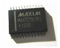
 MAX7219驱动8段数码管详解及数据手册关键信息

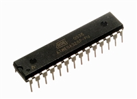
 ATMEGA328P技术资料深入分析

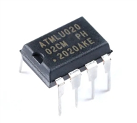
 AT24C02芯片手册管脚信息、参数分析、应用领域详解

 AT24C256芯片手册参数分析、引脚说明、读写程序示例
