ADMCF341
The processor contains three independent computational units:
the arithmetic and logic unit (ALU), the multiplier/accumulator
(MAC), and the shifter. The computational units process 16-bit
data directly and have provisions to support multiprecision
computations. The ALU performs a standard set of arithmetic
and logic operations as well as provides support for division
primitives. The MAC performs single-cycle multiply, multiply/add,
and multiply/subtract operations with 40 bits of accumulation.
The shifter performs logical and arithmetic shifts, normalization,
denormalization, and derive-exponent operations. The shifter
can be used to efficiently implement numeric format control,
including floating-point representations. The internal result (R)
bus directly connects the computational units so that the output
of any unit may be the input of any unit on the next cycle.
modes of operation. Serial port 1 (SPORT1) is available with a
limited number of I/Os. It is mainly intended for codebooting to
serial ROMs (SROM) and support of the debugging tools.
SPORT0 and SPORT1 can generate an internal programmable
serial clock or accept an external serial clock.
A programmable interval counter is also included in the DSP
core and can be used to generate periodic interrupts. A 16-bit
count register (TCOUNT) is decremented every n processor
cycles, where n – 1 is a scaling value stored in the 8-bit TSCALE
register. When the value of the counter reaches zero, an inter-
rupt is generated, and the count register is reloaded from a
16-bit period register (TPERIOD).
The ADMCF341 instruction set provides flexible data moves
and multifunction (one or two data moves with a computation)
instructions. Each instruction is executed in a single 50 ns
processor cycle (for a 10 MHz CLKIN). The ADMCF341
assembly language uses an algebraic syntax for ease of coding
and readability. A comprehensive set of development tools
supports program development. For further information on the
DSP core, refer to the ADSP-2100 Family User’s Manual, Third
Edition, with particular reference to the ADSP-2171.
A powerful program sequencer and two dedicated data address
generators ensure efficient delivery of operands to these compu-
tational units. The sequencer supports conditional jumps and
subroutine calls and returns in a single cycle. With internal loop
counters and loop stacks, the ADMCF341 executes looped code
with zero overhead; no explicit jump instructions are required to
maintain the loop.
Two data address generators (DAGs) provide addresses for
simultaneous dual operand fetches from data memory and pro-
gram memory. Each DAG maintains and updates four address
pointers (I registers). Whenever the pointer is used to access
data (indirect addressing), it is post-modified by the value in
one of four modifications (M registers). A length value may be
associated with each pointer (L registers) to implement auto-
matic modulo addressing for circular buffers. The circular
buffering feature is also used by the serial ports for automatic
data transfers to and from on-chip memory. DAG1 generates
only data memory addresses and provides an optional bit-reversal
capability. DAG2 may generate either program or data memory
addresses but has no bit-reversal capability. Efficient data trans-
fer is achieved with the use of five internal buses:
SERIAL PORTS
The ADMCF341 incorporates two complete synchronous serial
ports (SPORT1 and SPORT0) for serial communication and
multiprocessor communication.
Following is a brief list of capabilities of the ADMCF341
SPORTs. Refer to the ADSP-2100 Family User’s Manual, Third
Edition, for further details.
∑
∑
∑
SPORTs are bidirectional and have a separate, double-buff-
ered transmit and receive section.
SPORTs use an external serial clock or generate their own
serial clock internally.
SPORTs have independent framing for the receive and
transmit sections. Sections run in a frameless mode or with
frame synchronization signals internally or externally gener-
ated. Frame synchronization signals are active high or
inverted, with either of two pulsewidths and timings.
∑
∑
∑
∑
∑
Program memory address (PMA) bus
Program memory data (PMD) bus
Data memory address (DMA) bus
Data memory data (DMD) bus
Result (R) bus
∑
SPORTs support serial data word lengths from 3 bits to
16 bits and provides optional A-law and m-law companding
according to ITU (formerly CCITT) recommendation
G.711.
Program memory can store both instructions and data, permit-
ting the ADMCF341 to fetch two operands in a single cycle—
one from program memory and one from data memory. The
ADMCF341 can fetch an operand from on-chip program
memory and the next instruction in the same cycle. The
ADMCF341 writes data from its 16-bit registers to the 24-bit
program memory using the PX register to provide the lower 8
bits. When it reads data (not instructions) from 24-bit program
memory to a 16-bit data register, the lower 8 bits are placed in
the PX register.
∑
∑
SPORT receive and transmit sections can generate unique
interrupts on completing a data word transfer.
SPORTs can receive and transmit an entire circular buffer
of data with only one overhead cycle per data word. An
interrupt is generated after a data buffer transfer.
∑
∑
∑
SPORT0 has a multichannel interface to selectively receive
and transmit a 24-word, or 32-word, timedivision multi-
plexed, serial bitstream.
The ADMCF341 can respond to a number of distinct DSP
core and peripheral interrupts. The DSP interrupts comprise a
serial port receive interrupt, a serial port transmit interrupt, a
timer interrupt, and two software interrupts. Additionally, the
motor control peripherals include two PWM interrupts and a
PIO interrupt.
SPORT0 can be configured as an SPI port (master mode
only). The clock phase and polarity are programmable
through the MODECTRL register.
SPORT1 is the default port for program/data memory boot
loading and for development tools interface. The DT1/FL1
pin can be configured as SROM/E2PROM reset signal.
Serial port 0 (SPORT0) provides a complete synchronous serial
interface with optional companding in hardware and a wide
variety of framed and unframed data transmit and receive
–8–
REV. 0


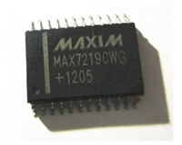
 MAX7219驱动8段数码管详解及数据手册关键信息

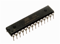
 ATMEGA328P技术资料深入分析

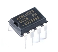
 AT24C02芯片手册管脚信息、参数分析、应用领域详解

 AT24C256芯片手册参数分析、引脚说明、读写程序示例
