ADM1067
Unlike some EEPROM devices that limit block writes to within
a page boundary, there is no limitation on the start address
when performing a block write to EEPROM, except when
•
To set up a 2-byte EEPROM address for a subsequent read,
write, block read, block write, or page erase. In this case,
the command byte is the high byte of the EEPROM address
from 0xF8 to 0xFB. The only data byte is the low byte of
the EEPROM address, as shown in Figure 36.
•
There must be at least N locations from the start address to
the highest EEPROM address (0xFBFF), to avoid writing to
invalid addresses.
1
2
3
4
5
6
7
8
EEPROM
ADDRESS
HIGH BYTE
(0xF8 TO 0xFB)
EEPROM
ADDRESS
LOW BYTE
(0x00 TO 0xFF)
•
An addresses cross a page boundary. In this case, both
pages must be erased before programming.
SLAVE
ADDRESS
S
W
A
A
A
P
Figure 36. Setting an EEPROM Address
Note that the ADM1067 features a clock extend function for
writes to EEPROM. Programming an EEPROM byte takes
approximately 250 μs, which limits the SMBus clock for repeated
or block write operations. The ADM1067 pulls SCL low and
extends the clock pulse when it cannot accept any more data.
Because a page consists of 32 bytes, only the 3 MSBs of the
address low byte are important f or page erasure. The lower
five bits of the EEPROM address low byte specify the
addresses within a page and are ignored during an erase
operation.
READ OPERATIONS
•
To write a single byte of data to EEPROM. In this case, the
command byte is the high byte of the EEPROM address
from 0xF8 to 0xFB. The first data byte is the low byte of the
EEPROM address, and the second data byte is the actual
data, as shown in Figure 37.
The ADM1067 uses the following SMBus read protocols.
Receive Byte
In a receive byte operation, the master device receives a single
byte from a slave device, as follows:
1
2
3
4
5
6
7
8
9
10
1. The master device asserts a start condition on SDA.
EEPROM
ADDRESS
HIGH BYTE
(0xF8 TO 0xFB)
EEPROM
ADDRESS
LOW BYTE
(0x00 TO 0xFF)
SLAVE
ADDRESS
2. The master sends the 7-bit slave address followed by the
read bit (high).
S
W
A
A
A
DATA
A
P
Figure 37. Single Byte Write to EEPROM
3. The addressed slave device asserts ACK on SDA.
4. The master receives a data byte.
Block Write
In a block write operation, the master device writes a block of
data to a slave device. The start address for a block write must
have been set previously. In the ADM1067, a send byte opera-
tion sets a RAM address, and a write byte/word operation sets
an EEPROM address, as follows:
5. The master asserts no acknowledge on SDA.
6. The master asserts a stop condition on SDA, and the
transaction ends.
In the ADM1067, the receive byte protocol is used to read a
single byte of data from a RAM or EEPROM location whose
address has previously been set by a send byte or write
byte/word operation, as shown in Figure 39.
1. The master device asserts a start condition on SDA.
2. The master sends the 7-bit slave address followed by
the write bit (low).
1
2
3
4
5
6
3. The addressed slave device asserts ACK on SDA.
4. The master sends a command code that tells the slave
device to expect a block write. The ADM1067 command
code for a block write is 0xFC (1111 1100).
5. The slave asserts ACK on SDA.
6. The master sends a data byte that tells the slave device how
many data bytes are being sent. The SMBus specification
allows a maximum of 32 data bytes in a block write.
7. The slave asserts ACK on SDA.
SLAVE
S
R
A
DATA
A
P
ADDRESS
Figure 39. Single Byte Read from EEPROM or RAM
Block Read
In a block read operation, the master device reads a block of
data from a slave device. The start address for a block read must
have been set previously. In the ADM1067, this is done by a
send byte operation to set a RAM address, or a write byte/word
operation to set an EEPROM address. The block read operation
itself consists of a send byte operation that sends a block read
command to the slave, immediately followed by a repeated start
and a read operation that reads out multiple data bytes, as
follows:
8. The master sends N data bytes.
9. The slave asserts ACK on SDA after each data byte.
10. The master asserts a stop condition on SDA to end the
transaction.
1
2
3
4
5
6
7
8
9
10
P
SLAVE
ADDRESS
COMMAND 0xFC
(BLOCK WRITE)
BYTE
COUNT
DATA
1
DATA
2
DATA
A
N
S
W
A
A
A
A
A
Figure 38. Block Write to EEPROM or RAM
Rev. B | Page 30 of 32


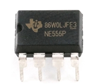
 解读NE555P资料手册:电气参数、引脚功能及替换型号推荐

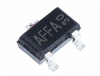
 AO3415资料解读:电气参数、替换型号推荐

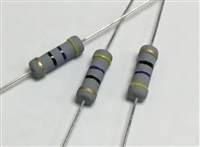
 电阻上的数字意义及电阻值辨别方法

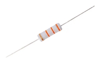
 金属氧化膜电阻器:定义、特点与深入解读
