
 5秒后页面跳转

| 是否无铅: | 不含铅 | 是否Rohs认证: | 符合 |
| 生命周期: | Active | 零件包装代码: | QFN |
| 包装说明: | HVQCCN, LCC60,.35SQ,20 | 针数: | 60 |
| Reach Compliance Code: | compliant | ECCN代码: | EAR99 |
| HTS代码: | 8542.39.00.01 | Factory Lead Time: | 1 week |
| 风险等级: | 1.26 | 最大模拟输入电压: | 2 V |
| 最小模拟输入电压: | -2 V | 最长转换时间: | 0.138462 µs |
| 转换器类型: | ADC, PROPRIETARY METHOD | JESD-30 代码: | S-PQCC-N60 |
| JESD-609代码: | e3 | 长度: | 9 mm |
| 最大线性误差 (EL): | 0.0342% | 湿度敏感等级: | 3 |
| 模拟输入通道数量: | 4 | 位数: | 12 |
| 功能数量: | 1 | 端子数量: | 60 |
| 最高工作温度: | 85 °C | 最低工作温度: | -40 °C |
| 输出位码: | BINARY | 输出格式: | SERIAL |
| 封装主体材料: | PLASTIC/EPOXY | 封装代码: | HVQCCN |
| 封装等效代码: | LCC60,.35SQ,20 | 封装形状: | SQUARE |
| 封装形式: | CHIP CARRIER, HEAT SINK/SLUG, VERY THIN PROFILE | 峰值回流温度(摄氏度): | 260 |
| 电源: | 3.3 V | 认证状态: | Not Qualified |
| 采样速率: | 65 MHz | 采样并保持/跟踪并保持: | SAMPLE |
| 座面最大高度: | 0.8 mm | 子类别: | Analog to Digital Converters |
| 最大压摆率: | 200 mA | 标称供电电压: | 3.3 V |
| 表面贴装: | YES | 技术: | CMOS |
| 温度等级: | INDUSTRIAL | 端子面层: | Matte Tin (Sn) |
| 端子形式: | NO LEAD | 端子节距: | 0.5 mm |
| 端子位置: | QUAD | 处于峰值回流温度下的最长时间: | NOT SPECIFIED |
| 宽度: | 9 mm | Base Number Matches: | 1 |
| 型号 | 品牌 | 获取价格 | 描述 | 数据表 |
| ADC12QS065CISQ/NOPB | TI |
获取价格 |
四通道、12 位、65MSPS 模数转换器 (ADC) | NKA | 60 | -40 |

|
| ADC12QS065CIVS | NSC |
获取价格 |
Quad 12-Bit 65 MSPS A/D Converter with LVDS Serialized Outputs |
|
| ADC12QS065EVAL | NSC |
获取价格 |
Quad 12-Bit 65 MSPS A/D Converter with LVDS Serialized Outputs |
|
| ADC-12QU/BCD | ADI |
获取价格 |
IC 1-CH 12-BIT PROPRIETARY METHOD ADC, PARALLEL ACCESS, DMA72, MODULE-72, Analog to Digita |
|
| ADC-12QU/BIN | ADI |
获取价格 |
IC 1-CH 12-BIT PROPRIETARY METHOD ADC, PARALLEL ACCESS, DMA72, MODULE-72, Analog to Digita |
|
| ADC-12QZ | ADI |
获取价格 |
IC 1-CH 12-BIT SUCCESSIVE APPROXIMATION ADC, PARALLEL ACCESS, DMA72, MODULE-72, Analog to |
|
| ADC-12QZ-003 | ADI |
获取价格 |
IC 1-CH 12-BIT SUCCESSIVE APPROXIMATION ADC, PARALLEL ACCESS, XMA, Analog to Digital Conve |
|
| ADC-12QZ-023 | ADI |
获取价格 |
IC 1-CH 12-BIT SUCCESSIVE APPROXIMATION ADC, PARALLEL ACCESS, XMA, Analog to Digital Conve |
|
| ADC12SJ1600 | TI |
获取价格 |
ADC12xJ1600 Quad, Dual, or Single Channel 1.6-GSPS, 12-Bit, Analog-to-Digital Converter (A |
|
| ADC12SJ1600AAV | TI |
获取价格 |
ADC12xJ1600 Quad, Dual, or Single Channel 1.6-GSPS, 12-Bit, Analog-to-Digital Converter (A |
|
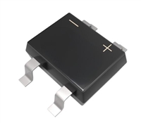 数据手册解读:MB10S引脚说明、电气参数

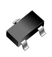 2N7002K资料解读:产品特性和型号推荐
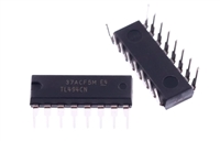 资料解读:TL494CN参数和引脚功能图说明
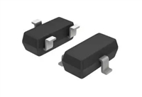 解读BAT54A数据手册:全面解析产品特性与应用
工作时间:9:00-21:00
CEO邮箱:ceo@jiepei.com
投诉邮箱:tousu@jiepei.com


 浙公网安备 33010502006866号 浙ICP备10014259号-119
营业执照ICP证
浙公网安备 33010502006866号 浙ICP备10014259号-119
营业执照ICP证


