AD7367
Preliminary Technical Data
tied to either a low or high logic state for the part to operate.
Suitable reference sources for the AD7367 include AD780,
AD1±82, ADR431, REF193, and ADR391.
VDRIVE
The AD7367 also has a ꢀDRIꢀE feature to control the voltage at
which the serial interface operates. ꢀDRIꢀE allows the ADC to
easily interface to both 3 ꢀ and ± ꢀ processors. For example, if
the AD7367 was operated with a ꢀCC of ± ꢀ, the ꢀDRIꢀE pin could
be powered from a 3 ꢀ supply, allowing a large dynamic range
with low voltage digital processors. Thus, the AD7367 could be
used with the ±10 ꢀ input range while still being able to
interface to 3 ꢀ digital parts.
The internal reference circuitry consists of a 2.± ꢀ band gap
reference and a reference buffer. When operating the AD7367
in internal reference mode, the 2.± ꢀ internal reference is
available at DCAPA and DCAPB pins, which should be decoupled
to AGND using a 680nF capacitor. It is recommended that the
internal reference be buffered before applying it elsewhere in
the system. The internal reference is capable of sourcing up to
1±0 μA with an analog input range of ±10 and 60 μA for both
the ±±ꢀ and 0-10ꢀ ranges.
To achieve the maximum throughput rate of 1Msps ꢀDRIꢀE must
be greater than or equal to 4.7±ꢀ, see table 3. The maximum
throughput rate for the AD7367 with the ꢀDRIꢀE voltage set to
less than 4.7± and greater than 2.7 is 900 Ksps.
If the internal reference operation is required for the ADC
conversion, the REFSEL pin must be tied to logic high on
power-up. The reference buffer requires ±00 µs to power up and
charge the 680nF decoupling capacitor during the power-up
time.
REFERENCE
The AD7367 can operate with either the internal 2.± ꢀ on-chip
reference or an externally applied reference. The logic state of
the REFSEL pin determines whether the internal reference is
used. The internal reference is selected for both ADC when the
REFSEL pin is tied to logic high. If the REFSEL pin is tied to
GND then an external reference can be supplied through the
DCAPA and DCAPB pins. On power-up, the REFSEL pin must be
The AD7367 is specified for a 2.± ꢀ to 3 ꢀ reference range.
When a 3ꢀ reference is selected, the ranges are ±12 ꢀ, ±6 ꢀ, and
0 ꢀ to +12 ꢀ. For these ranges, the ꢀDD and ꢀSS supply must be
equal to or greater than the +12ꢀ &-12ꢀ respectively.
Rev. PrD | Page 12 of 16


 AT24C256芯片手册参数分析、引脚说明、读写程序示例

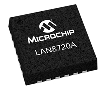
 LAN8720A的替代型号推荐、资料手册数据分析、特点介绍

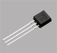
 SS8550数据手册:应用场景、主要参数分析、特性分析

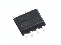
 UC3845全面解析:资料手册参数、引脚详解、维修技巧与替代型号推荐
