
| 型号 | 品牌 | 获取价格 | 描述 | 数据表 |
| 8SLVP2108_16 | IDT |
获取价格 |
Low Phase Noise, Dual 1-to-8, 3.3V, 2.5V LVPECL Output Fanout Buffer |

|
| 8SLVS1118 | IDT |
获取价格 |
LVDS/ LVPECL Fanout Buffer |
|
| 8SLVS1118 | RENESAS |
获取价格 |
1:18, 2.5V, 3.3V Selectable LVPECL or LVDS Fanout Buffer |
|
| 8SLVS1118NLGI | IDT |
获取价格 |
LVDS/ LVPECL Fanout Buffer |
|
| 8SLVS1118NLGI8 | IDT |
获取价格 |
LVDS/ LVPECL Fanout Buffer |
|
| 8SOIC | SMSC |
获取价格 |
8 PIN SOIC PACKAGE OUTLINE |
|
| 8SP208 | ETC |
获取价格 |
ALARM CONTROL PANEL |
|
| 8SP36-01-1-03N-F | GRAYHILL |
获取价格 |
Rotary Switch, 3 Positions, SP3T, Maintained, 0.25A, 28VDC, 12 PCB Hole Cnt, Solder Termin |
|
| 8SP36-01-1-04N-F | GRAYHILL |
获取价格 |
Rotary Switch, 4 Positions, SP4T, Maintained, 0.25A, 28VDC, 12 PCB Hole Cnt, Solder Termin |
|
| 8SP36-02-1-05S-F | GRAYHILL |
获取价格 |
Rotary Switch, 5 Positions, DP5T, Maintained, 0.25A, 28VDC, 12 PCB Hole Cnt, Solder Termin |
|
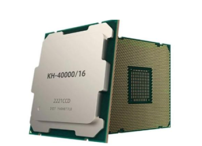 国产x86处理器里程碑!兆芯6000台医疗电脑中标某总医院

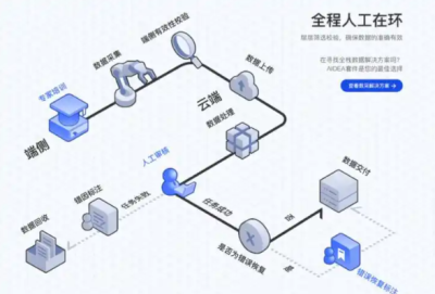 稚晖君团队开源GO-1模型:ViLLA架构如何重塑具身智能未来?
 安森美收购奥拉半导体Vcore技术 抢占AI数据中心电源管理制高点
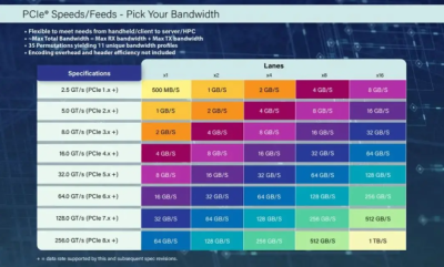 PCIe 8.0规范草案获里程碑进展:256GT/s速率开启1TB/s带宽时代
工作时间:9:00-21:00
CEO邮箱:ceo@jiepei.com
投诉邮箱:tousu@jiepei.com


 浙公网安备 33010502006866号 浙ICP备10014259号-119
营业执照ICP证
浙公网安备 33010502006866号 浙ICP备10014259号-119
营业执照ICP证


