
| 是否Rohs认证: | 符合 | 生命周期: | Transferred |
| 零件包装代码: | SON | 包装说明: | VSON, SOLCC6,.04,20 |
| 针数: | 6 | Reach Compliance Code: | compliant |
| HTS代码: | 8542.39.00.01 | 风险等级: | 5.12 |
| 系列: | AUP/ULP/V | JESD-30 代码: | R-PDSO-N6 |
| JESD-609代码: | e3 | 长度: | 1.45 mm |
| 负载电容(CL): | 30 pF | 逻辑集成电路类型: | LOGIC CIRCUIT |
| 最大I(ol): | 0.0017 A | 湿度敏感等级: | 1 |
| 功能数量: | 1 | 端子数量: | 6 |
| 最高工作温度: | 125 °C | 最低工作温度: | -40 °C |
| 封装主体材料: | PLASTIC/EPOXY | 封装代码: | VSON |
| 封装等效代码: | SOLCC6,.04,20 | 封装形状: | RECTANGULAR |
| 封装形式: | SMALL OUTLINE, VERY THIN PROFILE | 包装方法: | TAPE AND REEL |
| 峰值回流温度(摄氏度): | 260 | 电源: | 1.2/3.3 V |
| Prop。Delay @ Nom-Sup: | 22.3 ns | 认证状态: | Not Qualified |
| 施密特触发器: | YES | 座面最大高度: | 0.5 mm |
| 子类别: | Gates | 最大供电电压 (Vsup): | 3.6 V |
| 最小供电电压 (Vsup): | 0.8 V | 标称供电电压 (Vsup): | 1.1 V |
| 表面贴装: | YES | 技术: | CMOS |
| 温度等级: | AUTOMOTIVE | 端子面层: | Tin (Sn) |
| 端子形式: | NO LEAD | 端子节距: | 0.5 mm |
| 端子位置: | DUAL | 处于峰值回流温度下的最长时间: | 30 |
| 宽度: | 1 mm | Base Number Matches: | 1 |
| 型号 | 品牌 | 获取价格 | 描述 | 数据表 |
| 74AUP1G57GMAC | NXP |
获取价格 |
Low-power configurable multiple function gate |

|
| 74AUP1G57GN | NXP |
获取价格 |
Low-power configurable multiple function gate |
|
| 74AUP1G57GN | NEXPERIA |
获取价格 |
Low-power configurable multiple function gateProduction |
|
| 74AUP1G57GN,132 | NXP |
获取价格 |
74AUP1G57 - Low-power configurable multiple function gate SON 6-Pin |
|
| 74AUP1G57GNAC | NXP |
获取价格 |
Low-power configurable multiple function gate |
|
| 74AUP1G57GS | NXP |
获取价格 |
Low-power configurable multiple function gate |
|
| 74AUP1G57GS | NEXPERIA |
获取价格 |
Low-power configurable multiple function gateProduction |
|
| 74AUP1G57GSAC | NXP |
获取价格 |
Low-power configurable multiple function gate |
|
| 74AUP1G57GW | NXP |
获取价格 |
Low-power configurable multiple function gate |
|
| 74AUP1G57GW | NEXPERIA |
获取价格 |
Low-power configurable multiple function gateProduction |
|
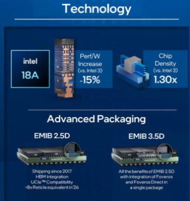 英特尔酷睿Ultra 300系列Panther Lake处理器深度解析:架构革新与AI性能飞跃

 美政府拟禁售TP-Link路由器 中国制造再遭"安全风险"围剿
 OpenAI豪掷数百亿美元绑定AMD 全球AI算力大战迎来新变局
 AMD与英特尔合作疑云:苏姿丰巧妙回应背后的美国制造战略
工作时间:9:00-21:00
CEO邮箱:ceo@jiepei.com
投诉邮箱:tousu@jiepei.com


 浙公网安备 33010502006866号 浙ICP备10014259号-119
营业执照ICP证
浙公网安备 33010502006866号 浙ICP备10014259号-119
营业执照ICP证


